
Circuit Diagram
Index 920
BIDIRECTIONAL_SWITCH
Published:2009/7/9 0:42:00 Author:May
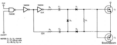
Using voltage doublers, this simple switch circuit uses a clock signal and a control signal to switch MOSFETs. (View)
View full Circuit Diagram | Comments | Reading(765)
10_volt_reference_with_4_ampere_capacity_using_an_AD581_and_a_2N6040
Published:2009/7/20 21:29:00 Author:Jessie
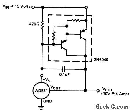
10-volt reference with 4-ampere capacity using an AD581 and a 2N6040 (courtesy Analog Devices, Inc.). (View)
View full Circuit Diagram | Comments | Reading(925)
SONAR_TRANSDUCER_SWITCH
Published:2009/7/9 0:42:00 Author:May
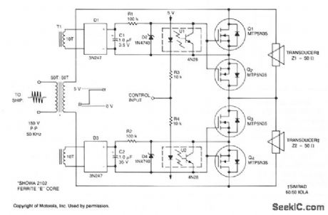
This submersible sonar positioning apparatus generally consists of dual-opposed ultrasonic transducers, alternately excited, with return signals processed and displayed for observation and measurement. Typical transmitter frequencies range from 50 to 200 kHz and pulse widths can be varied from 0.3 to 5 ms, depending on depth and resolution requirements.The input to the transducer/switch is transformer T1 which provides isolation and impedance matching. The turn ratio of the secondary windings depends on the peak-to-peak amplitude of the transmitter output into the specified load. The transmitted pulse that appears on the secondary winding charges capacitors C1 and C2 through bridge rectifiers D1 and D3. Zener diodes D2 and D4 limit the TMOS gate bias to 12 V; R1 and R2 limit the discharge current from C1 and C2.The square-wave control input is applied to opto-isolators U1 and U2 through resistors R3 and R4. If the control input is O V, U1 is activated; when it changes to + 5 V, U2 is activated. When U1 is activated, it saturates and reduces the gate bias to zero, turning Q1 and Q2 off. Q3 and Q4 remain on, effectively shunting transducer 22. When U2 is activated, it saturates and reduces the bias to zero, turning Q3 and Q4 off. Q1 and Q2 remain on, effectively shunting transducer Z1. (View)
View full Circuit Diagram | Comments | Reading(2484)
Power_supply_for_line_operated_servo_amplifier_using_a_power_transformer
Published:2009/7/20 21:28:00 Author:Jessie
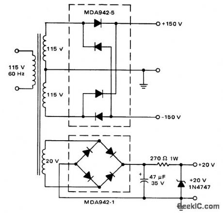
Power supply for line-operated servo amplifier using a power transformer (courtesy Motorola Semiconductor Products Inc.). (View)
View full Circuit Diagram | Comments | Reading(496)
LATCHING_ac_SOLID_STATE_RELAY
Published:2009/7/9 0:41:00 Author:May

Latching is obtained by storing the gate trigger energy from the preceding half cycle in the capacitors. Power must be interrupted for more than one full cycle of the line to ensure turn-off. Resistor R and capacitor C are chosen to minimize dissipation, while assuring triggering of the respective SCRs for each cycle. A pulse of current, over 10 ms duration into the H11C4 IRED, ensures triggering the latching relay into conduction. (View)
View full Circuit Diagram | Comments | Reading(1265)
AUTOMATIC_FRINGE_TUNING
Published:2009/7/20 21:06:00 Author:Jessie


Circuit serves to disable sound track, to increase amplitude of sound carrier, so weak picture car tier will be tuned higher on i-f pass band, at point of desired fringe tuning.-C. W. Baugh, Jr. and L. J. Sienkiewicz, Sound Signal Tunes Tv Automatically, Electronics, 31:17, p 54-58. (View)
View full Circuit Diagram | Comments | Reading(542)
24_volt_DC_regulated_power_supply_with_500_mA_rating
Published:2009/7/20 21:06:00 Author:Jessie
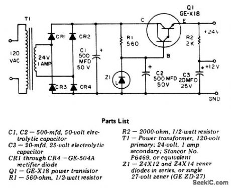
24-volt DC regulated power supply with 500 mA rating. Output ripple is less than 4.5 mV. R2 can be changed to obtain other secondary output voltages as desired (courtesy General Electric Company). (View)
View full Circuit Diagram | Comments | Reading(650)
ULTRASONIC_TRANSCEIVER
Published:2009/7/9 0:35:00 Author:May
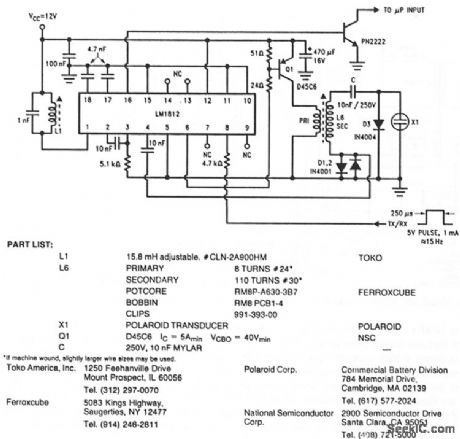
The LM1812 is a complete ultrasonic transceiver on a chip designed for use in a variety of pulseecho ranging applications. The chip operates by transmitting a burst of oscillations with a transducer, then using the same transducer to listen for a return echo. If an echo of sufficient amplitude is received, the LM1812 detector puts out a pulse of approximately the same width as the original burst. The closer the reflecting object, the earlier the return echo. Echos could be received immediately after the initial burst was trans-mitted, except for the fact that the transducer rings.
When transmitting, the transducer is excited with several hundred volts peak to peak, and it operates in a loudspeaker mode. Then, when the LM1812 stops transmitting and begins to receive, the transducer continues to vibrate or ring, even though excitation has stopped. The transducer acts as a microphone and produces an ac signal initially the same amplitude as the transmit pulse. This signal dies away as is gov-erned by the transducer's damping factor, but as long as detectable ringing remains, the LM1812's detector will be held on, masking any return echos. (View)
View full Circuit Diagram | Comments | Reading(1997)
SLIDING_GATE_FOR_HEART_SOUNDS
Published:2009/7/20 21:05:00 Author:Jessie

Two multivibrators, synchronized with time reference,permit listening to selected portions of heart sound. Potentiometers permit adjusting width and position of gate.-R. Weiss, Heart-Sound Discriminator Simplifies Medical Diagnosis, Electronics, 34;24, p 52-55. (View)
View full Circuit Diagram | Comments | Reading(807)
FOURTH_ORDER_100_Hz_HIGH_PASS_FILTER
Published:2009/7/9 0:05:00 Author:May

This filter, using two sections of LM741, can be scaled in frequency ,If desired. (View)
View full Circuit Diagram | Comments | Reading(1130)
300_TO_3400Hz_SECOND_ORDER_SPEECH_FILTER
Published:2009/7/9 0:03:00 Author:May

Using two op amps,this filter is designed for second-order response.It has a bandpass of 300 to 3 400Hz,for applications In speech or telephone work. (View)
View full Circuit Diagram | Comments | Reading(2100)
VOCAL_ELIMINATOR
Published:2009/7/9 0:02:00 Author:May

Otherwise properly mixed sounds often suffer from a predominant solo voice (which might, of course, be the intention). If such a voice needs to be suppressed, the present circuit will do the job admirably.
The circuit is based on the fact that solo voices are invariably situated at the center of the stereo recordings that are to be mixed. Thus, voice levels in the left-and right-hand channels are about equal. Arithmetically, therefore, left minus right equals zero; that is, a mono signal without voice.
There is, however, a problem: the sound levels of bass instruments, more particularly the double basses, are also just about the same in the two channels. On the one hand low-frequency sounds are virtu-ally nondirectional and on the other hand, the recording engineers purposely use these frequencies to give a balance between the two channels.
However, the bass instruments can be recovered by adding those appearing in the left+right signal to the left-right signal. The whole procedure is easily followed in the circuit diagram. The incoming stereo signal is buffered by Al and A2. The buffered signal is then fed to differential amplifier A3 and subse-quently to summing amplifier A5. The latter is followed by a low-pass filter formed by A6. You can choose between a first-order and a second-order filter by respectively omitting or fitting C2. Listen to what sounds best.
The low-frequency signal and the difference signal are applied to summing amplifier A4. The balance between the two is set by P1 and P2 to individual taste.
You have noticed that the circuit does not contain input or output capacitors. If you wish, output capac-itors can be added without detriment. However, adding input capacitors is not advisable, because the con-sequent phase shift would adversely affect the circuit operation. (View)
View full Circuit Diagram | Comments | Reading(1491)
DIODE_MIXER_FOR_TUNER
Published:2009/7/20 21:05:00 Author:Jessie

1N87 semiconductor diode mixer D1 improves isolation of r-f amplifier from 6ER5 tube V2, connected as Colpitts oscillator.-E. H. Hugenholtz, 0ne-Tube Oscillator Mixers for Tv and F-M Tuners, Electronics, 33:3, p 76-79. (View)
View full Circuit Diagram | Comments | Reading(611)
LOW_FTEQUENCY_MULTIPLIER
Published:2009/7/9 0:01:00 Author:May


This circuit uses a comparator as a Schmitt trigger (311H) and two active bandpass filters LM318H).3-kHz output is obtained. Higher harmonics (preferably odd) can be obtained by tuning the active filters to the desired frequency.N can be 1, 3, 5, 7, 9, etc. Even harmonics can be produced by substituting a full-wave rectifier or absolute-value circuit for the Schmitt-trigger comparator. (View)
View full Circuit Diagram | Comments | Reading(1027)
TWO_SECTION_300_3000Hz_SPEECH_FILTER
Published:2009/7/9 0:01:00 Author:May

An LM387 dual low-noise amplifier is used in an active filter. Both sections are used to produce second-order HP and LP filters, respectively. (View)
View full Circuit Diagram | Comments | Reading(1601)
ANTIALASING_AND_SYNC_COMPENSATION_FILTER
Published:2009/7/8 23:58:00 Author:May

Two dual-biquad filter ciUps and some external components form a multipurpose filter to reconstruct D/A converter signals. Connected to a converter’s output, the filter provides antialiasing, reduces the D/A converter’s quantization noise, and compensates for sin(πx) ÷ (πx)-the sync function (attenuation).
The circuit incorporates an inverse-sync function that operates to one-third of the converter’s sample rate. Beyond one-third, the filter’s response shifts to a stopband filter, which provides -70 dB attenua-tion. This attenuation conforms to the converter’s inherent signal-to-noise ratio and quantization error.
To prevent aliasing, the stopband edge must be no higher than the Nyquist frequency (fsn÷2). To achieve 70-dB stopband rejection with this eighth-order filter requires a transition ratio (fSTOPgAND÷fPASSsAND) of 1.5, which sets the passband’s upper limit at fS÷3.
Notice also that you can apply a simple divide-by-64 circuit to the 192-kHz clock frequency to set the necessary 3× ratio between the converter’s sample rate and the filter’s 1-kHz comer frequency. The V+, V-, and the FO through F5 connections program each filter chip for an fCLK/f0 ratio of 191.64. (View)
View full Circuit Diagram | Comments | Reading(820)
AUDIO_EQUALZER
Published:2009/7/8 23:58:00 Author:May

Designed for communications use, this equalizer circuit uses a Mitsubishi M5226P audio equalizer IC to adjust frequency response. It runs from a 9 to 20 V supply. C6 through C16 are polyester film capacitors of ± 5% tolerance. (View)
View full Circuit Diagram | Comments | Reading(4696)
Variable_output_voltage_regulator_using_the_μA79HG_which_can_supply_a_minimum_of_5_amperes_at_voltages_from__23_volts_to__24_volts
Published:2009/7/20 21:05:00 Author:Jessie

Variable output voltage regulator using the μA79HG, which can supply a minimum of 5 amperes at voltages from -2.3 volts to -24 volts (courtesy Fairchild Semiconductor). (View)
View full Circuit Diagram | Comments | Reading(569)
VIDEO_OUTPUT_AMP
Published:2009/7/20 21:04:00 Author:Jessie
With 2N834 circuit, output is sufficient to drive crt.-W. D, Roehr, Epitaxial Process Improves Transistor Charateristics, Electronics, 34:9, p 52-53. (View)
View full Circuit Diagram | Comments | Reading(600)
CABLE_TESTER
Published:2009/7/20 21:04:00 Author:Jessie

Five Signetics NE555V timers check all lines of four-conductor cable for opens and for short-circuit conditions, Differential transistor pall at one end of each cable line remains balanced as long as clock pulses at opposite ends of line are identical. Clock pulse at timer end of one line turns on green LED to indicate open in line. Clock pulse only at transistor end of line turns on red LED to indicate that line is shorted With good cable line, neither LED is on.- Signetics Analog Data Manual, signetics,Sunnyvale,CA,1977,p730. (View)
View full Circuit Diagram | Comments | Reading(0)
| Pages:920/2234 At 20901902903904905906907908909910911912913914915916917918919920Under 20 |
Circuit Categories
power supply circuit
Amplifier Circuit
Basic Circuit
LED and Light Circuit
Sensor Circuit
Signal Processing
Electrical Equipment Circuit
Control Circuit
Remote Control Circuit
A/D-D/A Converter Circuit
Audio Circuit
Measuring and Test Circuit
Communication Circuit
Computer-Related Circuit
555 Circuit
Automotive Circuit
Repairing Circuit