
Circuit Diagram
Index 907
PRECISION_FULL_WAVE_RECTFIER
Published:2009/7/9 2:45:00 Author:May
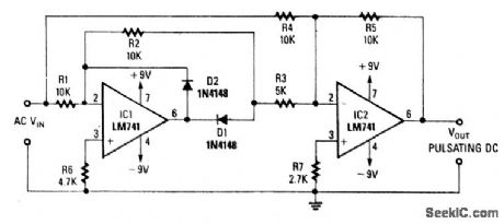
Using two op amps, this circuit produces a full-wave rectified version of the input signal. Op amp IC1 inverts the negative-going signal, but because of D2, it stays near zero. IC2 produces a positive-going sig-nal. For positive-going signals, IC1 produces a negative output through D1 to IC2, where it is combined with positive VIN from R4/R5. At the summing junction of IC2, the negative output of IC1 is doubled and inverted via IC2, R3, and R5 to produce + V0UT. This is summed with negative output of IC1 to produce + V0UT. (View)
View full Circuit Diagram | Comments | Reading(726)
DUAL_TRACKING_REGULATOR
Published:2009/7/9 2:45:00 Author:May
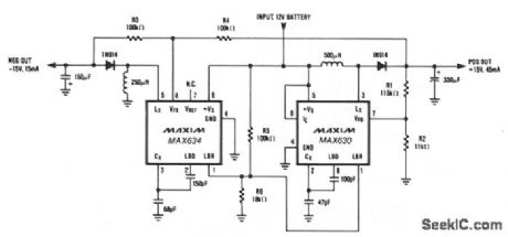
A MAX634 inverting regulator is combined with a MAX630 to provide a dual tracking ±5 output from a 12-V battery. The reference for the -15 V output is derived from the positive output via R3 and R4. Both regulators are set to maximize output power at low battery voltages by reducing the oscillator frequency, via LBR, when VBATT falls to 8.5V. (View)
View full Circuit Diagram | Comments | Reading(593)
LASER_TV
Published:2009/7/20 20:30:00 Author:Jessie
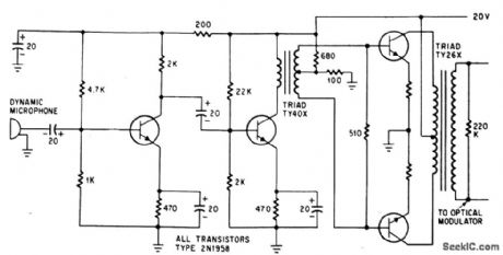
Audio driver delivers 300 v peak. to peak to KDP optical modulator controlling gas laser.-C. J. Peters et al., Laser-Television System Developed With Off-The Shelf Equipment, Electronics, 38:3, p 75-78.
(View)
View full Circuit Diagram | Comments | Reading(761)
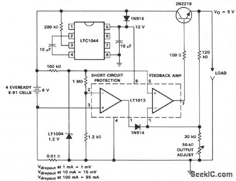
LOW_DROPOUT_5_V_REGULATOR
Published:2009/7/9 2:43:00 Author:May
View full Circuit Diagram | Comments | Reading(543)
SIMPLE_OP_AMP_AUDIO_AMPLIFIER
Published:2009/7/9 2:43:00 Author:May

A CA3140 drives a complementary output stage Q1, Q2, and Q3. Output power depends on supply voltage and limits on dissipations of Q2 and Q3, but it can be 1 or 2 W with a higher impedance speaker and a 30-V supply. (View)
View full Circuit Diagram | Comments | Reading(889)
RLC_BRIDGE
Published:2009/7/20 20:29:00 Author:Jessie

Maxwell bridge uses only one re-active element for measuring resistance, inductance, and capacitance. Wagner ground balances stray internal capacitances to ground to obtain perfect null. Measurement ranges are shown in table. 0ver fixed range, RA can be calibrated to read inductance values directly. RA and RB can be calibrated initially over their variable ranges by using standard resistors. Measurements are not affected by frequency of driving source. Circuit is set up as shown for measuring inductance. If standard inductance is used in place of Lx, unknown capacitor at CB can be measured. Signetics NE555 is connected as astable oscillator running at about 1000 Hz with values shown for R and C, drawing 6.5 mA from 9-V battery. Article covers construction and calibration and gives balance equations for all measurements.-J. Ii. Ellison, Universal L, C, R Bridge, Ham Radio, April 1976, p 54-55. (View)
View full Circuit Diagram | Comments | Reading(3456)
VIDEO_DC_RESTORER
Published:2009/7/9 2:42:00 Author:May
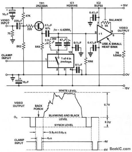
The main requirement for efficient dc restoration is to provide a short time-constant during the clamp period,with a long time-constant during the active line time.The switch within the Harris HI201HS has anon resistance of 30 Ω and the PMI buffer, BUF03,has an input resistance of 50 MΩ.The tuned circuit presents a high impedance at the 4.43-MHz color subcarrier frequency SO that the color-burst signal is retained if the video signal contains this information, (View)
View full Circuit Diagram | Comments | Reading(981)
HAND_HELD_TRANSCEIVER_DCADAPTER
Published:2009/7/9 2:41:00 Author:May
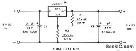
This dc adapter provides a regulated 9-V source for operating a Kenwood TR-2500 hand-held transceiver in the car. The LM317T's mounting tab is electrically connected to its output pin, so take this into account as you construct your version of the adapter. The LM317T regulator dissipates 2 or 3 W in this application, so mount it on a 1- x -2-inch piece of 1/8-inch-thick aluminum heatsink. (View)
View full Circuit Diagram | Comments | Reading(1930)
8_W_AUDIO_AMPLIFIER
Published:2009/7/9 2:41:00 Author:May
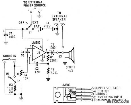
This audio power amp (built around an LM383 8-W, audio power amplifter) can be used to boost an audio signal to a sufficient level so that it can be heard in a high-noise environment. Note that LM383 should be heatsinked. (View)
View full Circuit Diagram | Comments | Reading(716)
AUTOMATIC_LOCAL_FRINGE_TUNING
Published:2009/7/20 20:28:00 Author:Jessie

Complele automatic fine tuning system com bines features of fringe switching and auto matic-manual operation. Switching transients are reduced by 180-mmfd capacitor-C. W. Baugh, Jr., and L. J. Sienkiewicz, Sound Signal Tunes Tv Automatically, Electronics, 31:17, p 54-58. (View)
View full Circuit Diagram | Comments | Reading(625)
LONG_NE_IR_DROP_VOLTAGE_RECOVERY
Published:2009/7/9 2:40:00 Author:May
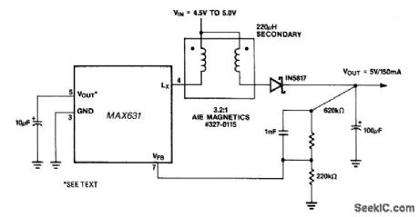
This circuit provides a unique solution to a common system-level power distribution problem: When the supply voltage to a remote board must traverse a long cable, the voltage at the end of the line some-times drops to unacceptable levels. This + 5-V/ + 5-V converter addresses this by taking the reduced volt-age at the end of the supply line and boosting it back to + 5 V. This can be especially useful in remote display devices, such as some point-of-sale (POS) terminals, where several meters of cable could separate the terminal from the readout. (View)
View full Circuit Diagram | Comments | Reading(510)
AUDIO_AMPLIFIER
Published:2009/7/9 2:40:00 Author:May
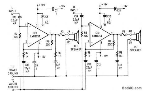
This amplifier will deliver around 20 W to an 8-Ω speaker. (View)
View full Circuit Diagram | Comments | Reading(0)
RECEIVER_AUDIO_CIRCUIT
Published:2009/7/9 2:37:00 Author:May
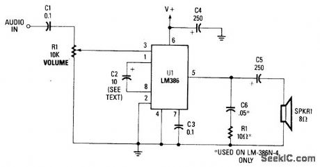
This simple receiver AF amplifier can supply several hundred milliwatts to an 8-Ω speaker. The gain is about 200X. If high gain is not needed, C2 can be deleted and a gain of 20 will be obtained. R1 and C6 are musts, otherwise ultrasonic (30 to 60 kHz) oscillations might occur. C6 can be 0.1 μF on all LM386N versions for protection against these oscillations. The supply voltage is typically 6 to 12 V. No heatsink is necessanr, but good grounding is a must. (View)
View full Circuit Diagram | Comments | Reading(1004)
OSTEOGRAPH_DETECTS_BONE_DISEASE
Published:2009/7/20 20:26:00 Author:Jessie
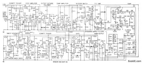
Electronic scanner using television fiying-spot microscope measures irregular micro-scopic tissue areas of spongy bone, for earlydiagnosis of bone disease. Television moni-tor receiver shows enktrged picture of bone section as ctid in centering areo to be scanned. Recorder plots ratio between bonearec and marrow area.-0. W. Jones III, R. V. Vreelcmd, and C. C. Collins, Video Microplanimeter Detects Bone Disease, Flee.tronics, 31:43, p 85-87. (View)
View full Circuit Diagram | Comments | Reading(1186)
107_MHz_IF_amplifier_using_a_3N204_dual_gate_MOSFET
Published:2009/7/20 20:25:00 Author:Jessie
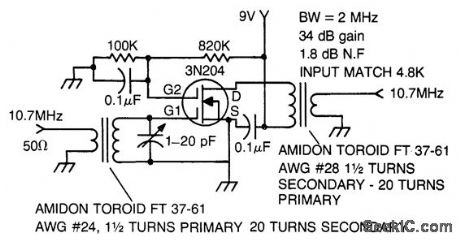
10.7 MHz IF amplifier using a 3N204 dual-gate MOSFET (courtesy Texas tnstruments tncorporated). (View)
View full Circuit Diagram | Comments | Reading(0)
ISOLATED_FEEDBACK_POWER_SUPPLY
Published:2009/7/9 2:37:00 Author:May

Figure 73-4 is a power supply circuit using the isolated feedback capabilities of the TL3103 for both current and voltage sensing. This supply is powered from the ac power line and has an output of 5 V at 1.5 A. Both output voltage and current are sensed and the error voltages are applied to the error amplifters of the TL594 PWM control IC. The 24-V transformer produces about 35 V at the 1000-μF filter capacitor. The 20-kHz switching frequency is set by the 6-KΩ resistor and the 0.01-μF capacitor on pins 6 and 5, respectively. The TL594 is set for push-pull operation by typing pin 13 high. The 5-V reference on pin 14 is tied to pin 15, which is the reference or the current error amplifier. The 5-V reference is also tied to pin 2 which is the reference for the output voltage error amplifier. The output voltage and current limit are set by adjustment of the 10-KΩ pots in the TL3103 error-sensing circuits. A pair of TIP31E npn transistors are used as switching transistors in a push-pull circuit. (View)
View full Circuit Diagram | Comments | Reading(2525)
PICTURE_FIXER_INVERTER
Published:2009/7/9 2:36:00 Author:May
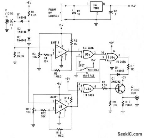
The circuit will accept a video signal, separate the sync pulses, invert the video, and add new video to the old sync pulses. The video signal is brought in through J1 and applied to a clamping circuit consisting of C1, D1, D2, D3, R1, and R2. The clamp circuit forces all of the sync pulses to align with the same dc voltage level. With the video voltage clamped, the trip points of the comparators that follow can be set with trimmer resistors R3 and R11. The resistors will not have to be readjusted. One comparator, U1, is adjusted to change states with a change in either video or sync-pulse levels. The other comparator, U2, is adjusted to trip on changes of sync-pulse levels only.The output of U1 now consists of a logic level, 0 to + 5 V, signal that contains both sync pulses and video. The composite signal is coupled to an EXCLUSIVE-OR gate, U3a, where it is either inverted or not inverted, depending upon the position of switch NORM/REV S1. The output, at pin 3 of U3a, is next sent to U3b. There the composite signal is combined with the sync-pulse only signal from U2. The EXCLUSIVE-OR action of U3b cancels out the sync pulses, leaving only video at the IC's output.Since the sync pulses are inverted as they pass through U2, they must be inverted once more before being combined with the video signal. That final inversion is performed by U3c, and that device's output is combined with that of U3b via D4, R7, R8, and R9. The newly combined signal is buffered by emitter-follower Q1, and sent to the outside world via J2. The circuit can be powered by a 9- to 12-V wall-mount power supply. The supply voltage is regulated down to 5 V by U4. (View)
View full Circuit Diagram | Comments | Reading(789)
BULL_HORN
Published:2009/7/9 2:36:00 Author:May
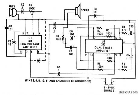
This bull horn uses U1 as a driver stage and U2 as an output driver. U1 is set up for a gain of 200. The microphone should have about 200-mVpp output. The two sections of U2 produce about 4-W of output power. Use shielded cable for all audio leads. Power is a 6-to 9-V battery or other source. (View)
View full Circuit Diagram | Comments | Reading(1298)
Frequency_synthesizer_mixer_for_BC_operation_using_a_dual_gate_3N204_dual_gate_MOSFET
Published:2009/7/20 20:24:00 Author:Jessie
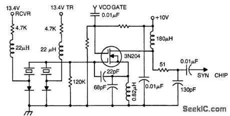
Frequency synthesizer mixer for BC operation using a dual-gate 3N204 dual-gate MOSFET (courtesy Texas Instruments Incorporated.). (View)
View full Circuit Diagram | Comments | Reading(1084)
VOLTAGE_DOUBLER
Published:2009/7/9 2:32:00 Author:May

This circuit drives relays of 24 and 18 Vdc from a 12-V power supply. Use this circuit with almost any pnp or npn power transistor.Parts: U1: NE 555 timer. C1 and C2: 50 μF/ 25 Vdc. Q1: TIP 29, TIP120, 2N4922, TIP61, TIP110, or 2N4921. Q2: TIP30, TIP125, 2N4919, TIP62, TIP115, or 2N4918. (View)
View full Circuit Diagram | Comments | Reading(1467)
| Pages:907/2234 At 20901902903904905906907908909910911912913914915916917918919920Under 20 |
Circuit Categories
power supply circuit
Amplifier Circuit
Basic Circuit
LED and Light Circuit
Sensor Circuit
Signal Processing
Electrical Equipment Circuit
Control Circuit
Remote Control Circuit
A/D-D/A Converter Circuit
Audio Circuit
Measuring and Test Circuit
Communication Circuit
Computer-Related Circuit
555 Circuit
Automotive Circuit
Repairing Circuit