
Circuit Diagram
Index 917
100_MHz_oscillator_and_buffer
Published:2009/7/20 23:17:00 Author:Jessie

100 MHz oscillator and buffer (courtesy Texas Instruments Incorporated). (View)
View full Circuit Diagram | Comments | Reading(737)
105_MHz_gate_1_contraolled_BF_amplifier_using_a_TIS152_dual_gate_MOSFET
Published:2009/7/20 23:15:00 Author:Jessie

105 MHz gate-1-contraolled BF amplifier using a TIS152 dual-gate MOSFET(courtesy Texas Instruments Incorporated). (View)
View full Circuit Diagram | Comments | Reading(563)
1_second_reference_oscillator
Published:2009/7/20 23:15:00 Author:Jessie

1-second reference oscillator. This circuit is ideal for clock circuits where no 60-hertz line is available (courtesy Intersil, Inc.). (View)
View full Circuit Diagram | Comments | Reading(813)
10_watt_and_25_watt_marine_bano_transmitters_
Published:2009/7/20 23:13:00 Author:Jessie

10-watt and 25-watt marine bano transmitters (courtesy Motorola Semiconductor Products Inc.). (View)
View full Circuit Diagram | Comments | Reading(480)
Watchdog_light_sensitive_oscillator
Published:2009/7/20 23:11:00 Author:Jessie

Watchdog light-sensitive oscillator. The basic circuit is a relaxation oscillator that sounds an alarm through a speaker or earphone. R2 is set for a bias current just below the firing level (courtesy General Electric Company). (View)
View full Circuit Diagram | Comments | Reading(1016)
25_watt_marine_band_transmitter
Published:2009/7/20 23:11:00 Author:Jessie


25-watt marine band transmitter. See page258 for parts list, (View)
View full Circuit Diagram | Comments | Reading(562)
Digital programmable voltage reference circuit diagram with 0 ~ 9.99V Output voltage
Published:2011/5/10 4:21:00 Author:Rebekka | Keyword: Digital programmable voltage reference, 0 ~ 9.99V output voltage

Figure shows the output voltage 0 ~ 9.99V digital programmable reference voltage source circuit. The circuit is composed of 12-bit D / A converter, DAC-80-CCD-V, VT1, VT2, the current amplifier and other components. The larger output current is, the more widespread use it will hace. But it is used for experiment and adjustment of the reference voltage source. The output current is 100mA. If the step voltage is set to be 1mV, you need to add an attenuator composed of the resistance Rl and R2. The output voltage is 0 ~ 9.99V. In Circuit, RPl is used for full-scale adjustment, RP2 is used for zero.
(View)
View full Circuit Diagram | Comments | Reading(1911)
Voltage_controlled_sine_wave_oscillator_for_up_to_50_kHz
Published:2009/7/20 23:10:00 Author:Jessie

Voltage-controlled sine-wave oscillator for up to 50 kHz. For frequencies of 10 kHz to 50 kHz capacitor Cc should be 3 pF. For frequencies less than 10 kHz capacitor Cc should be 30 pF. Select capacitor C according to desired frequency, or make it variable from zero to 5 μF (courtesy Fairchild Semiconductor). (View)
View full Circuit Diagram | Comments | Reading(1160)
UP_DOWN_RAMP_CONTROL
Published:2009/7/20 23:10:00 Author:Jessie


Siliconix DG387CJ solid-state relay A4 provides switch-ing from up ramp to down ramp for decelerating servo when it zeroes in on correct new position. Slopes are determined by settings of R1 and R2. Arrangement ensures optimum senro system response at low cost. A1 detects that input is other than 0 V and energizes optoisolator A3 for switching A4. Resulting positive-going ramp from A5 moves system load toward desired position, making feedback voltage of servo reduce control-input voltage. When this drops to within 0.7 V of ground, A1 goes low and A3 turns off. A4 now initiates down-ramp waveform to decelerate system to stop. For ramp rate of 20V/s, C can be 0.33μF and R3 1.8 megohms.-R.E. Kelly, Up-Down Ramp Quickens Servo System Response, Electronics, July 20, 1978, p 121 and 123. (View)
View full Circuit Diagram | Comments | Reading(994)
10_watt_marine_band_transmitters
Published:2009/7/20 23:08:00 Author:Jessie

10-watt marine band transmitters. See page-for parts list. (View)
View full Circuit Diagram | Comments | Reading(969)
200_MHz_crystal_oscillator
Published:2009/7/20 23:07:00 Author:Jessie

200 MHz crystal oscillator. This circuit incorporates a 100 MHz oscillator and a frequency doubler. VEE is -5.2 volts (courtesy Motorola Semiconductor Products Inc.). (View)
View full Circuit Diagram | Comments | Reading(1066)
DIFFERENTIAL_INPUT_AND_OUTPUT
Published:2009/7/20 23:07:00 Author:Jessie

Preamplifier for servo system uses 90° operational integrator to drive MC1420 opamp having differential input and differential output connected in inverting configuration. With values shown, voltage gain is about 38 dB. Bandwidth is about 4 kHz, giving stability when using 510-pF compensating capacitors. Zener provides 12 V required for opamp operation from single supply,-A, Pshaenich, Servo Motor Drive Amplifiers, Motorola, Phoenix, AZ, 1972, AN-590. (View)
View full Circuit Diagram | Comments | Reading(653)
High power DC motor over-current protection circuit diagram
Published:2011/8/2 2:56:00 Author:Rebekka | Keyword: High power DC, motor over-current protection
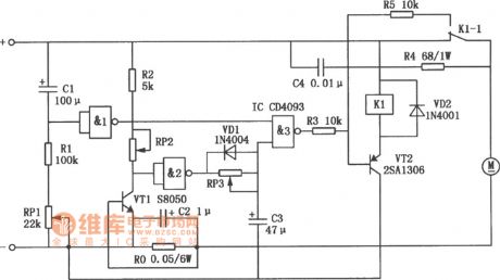
In order to prevent the motor generating high current and make the circuit work inappropriately. the Cl, Rl, RPl and NAND gate form the starting protection time delay circuit. When the motor starts, there is not voltage at Cl. At this time NAND gate 1 outputs low level, NAND gate 3 outputs high level, it makes the VT2 in the off mode, then the relay Kl does not work, andits contact stillkeeps the closed mode. The DC motor gets normal power supply. When the Cl terminal voltage rises gradually to a certain value, the NAND gate 1 is overturned, the output terminal turns to high level, the start protection circuit stops to work. After that the output mode of NAND gate 3 is the current detection circuit control composed of the RP2, R2, VTl and Ro. (View)
View full Circuit Diagram | Comments | Reading(3213)
20W_AT_60_Hz
Published:2009/7/20 22:55:00 Author:Jessie

Adding high-current oomph mentary transistors to opamp gives servoam-plifier with 115-V output. Opamp drives low impedance of 10-V filament transformer connected in reverse to boost output to 115 V for driving servo. Use heatsink for transistors. Bringing opamp feedback resistor to actual out-put point makes nonlinearities and crossover point between transistors insignificant by placing them in feedback loop.-I. Math, Math's Notes, CQ, Jan. 1978, p 53-54 and 70. (View)
View full Circuit Diagram | Comments | Reading(1710)
105_MHz_to_107_mixer_for_FM_operation
Published:2009/7/20 22:55:00 Author:Jessie

105 MHz to 10.7 mixer for FM operation (courtesy Texas Instruments Incorporated). (View)
View full Circuit Diagram | Comments | Reading(571)
Digitally_programmed_oscillator
Published:2009/7/20 22:54:00 Author:Jessie

Digitally programmed oscillator. The circuit uses an AD537 monolithic V/F converter and an AD7520 multiplying D/A convener. It is a programmable square wave frequency source with excellent linearity in the range of0 to 100 kHz (courtesy Analog Devices, Inc.). (View)
View full Circuit Diagram | Comments | Reading(653)
TWO_DOOR_ANNUNCIATOR
Published:2009/7/8 23:06:00 Author:May

When the pushbuttons at either door are depressed, this circuit generates a different tone for each door. Tones are generated by phase-shift oscillator Q1/Q2. Q3 provides tone frequency change by chang-ing the phase-shift network. U2 and U3 are timers for the tones and Q4/Q5 interface the timers with the pushbuttons. (View)
View full Circuit Diagram | Comments | Reading(747)
Quadrature_oscillator_using_an_ECG947_dual_operational_amplifier_IC
Published:2009/7/20 22:53:00 Author:Jessie

Quadrature oscillator using an ECG947 dual operational amplifier IC. The ECG947 is short-circuit proof and requires no external components for frequency compensation (courtesy GTE Sylvania Incorporated). (View)
View full Circuit Diagram | Comments | Reading(1266)
FIELD_STRENGTH_METER
Published:2009/7/8 23:06:00 Author:May

This field-strength meter is basically a bridge circuit that is equipped with a 0-to-1-mA meter as a readout. (View)
View full Circuit Diagram | Comments | Reading(0)
OPERATIONAL_INTEGRATOR_PHASE_SHIFTER
Published:2009/7/20 22:52:00 Author:Jessie

Motorola MPSA13 Darlington IC provides 90° phase shift required in servo amplifier for 115-V 60-Hz servomotor. Two cascaded 2N3904 discrete Darlingtons can be used in place of IC.-A. Pshaenich, Servo Motor Drive Amplifiers, Motorola. Phoenix, AZ, 1972, AN-590. (View)
View full Circuit Diagram | Comments | Reading(860)
| Pages:917/2234 At 20901902903904905906907908909910911912913914915916917918919920Under 20 |
Circuit Categories
power supply circuit
Amplifier Circuit
Basic Circuit
LED and Light Circuit
Sensor Circuit
Signal Processing
Electrical Equipment Circuit
Control Circuit
Remote Control Circuit
A/D-D/A Converter Circuit
Audio Circuit
Measuring and Test Circuit
Communication Circuit
Computer-Related Circuit
555 Circuit
Automotive Circuit
Repairing Circuit