
Circuit Diagram
Index 918
TREMOLO
Published:2009/7/8 23:05:00 Author:May

The VCO of U1, a phased-locked loop, produces a low-frequency square-wave signal from 5 Hz to 2500 Hz, which is controlled by varying the voltage to pin 9 via R2. The frequency threshold is set by R1 and C1. Increasing the value of R1 increases the frequency, and decreasing the value of C1 decreases the threshold frequency. Transistor Q1 is operated as an amplifier with the Q point at 4 V, using a transistor with a voltage gain (beta) of 100. The gain without tremolo is about 2 V. With bypass capacitor C4 in the circuit, the gain is set at 33 dB. The instrument drive cannot be greater than 30 mV with C4 in the circuit (no tremolo), to avoid distortion. Without C4, the drive can be 1.5 V maximum with no distortion. U1's output is coupled to the collector of transistor Q1 via depth control R4. The square-wave signal pulls the audio at a frequency determined by R2. The oscillator is activated by foot switch S1. (View)
View full Circuit Diagram | Comments | Reading(1034)
ELECTRONIC_BELL
Published:2009/7/8 23:02:00 Author:May

A 555 timer pulses twin-T oscillator Q1.Q2 acts as an output buffer.R7 adjusts the frequency of oscillator Q1. (View)
View full Circuit Diagram | Comments | Reading(0)
SCR_CIRCUIT_WITH_SELF_NTERRUPTING_LOAD
Published:2009/7/8 23:00:00 Author:May

A self-interrupting device connected to a volt-age source functions as a switch that repeatedly opens and closes; therefore, the circuit does not latch in the normal way, so the alarm operates only as long as S1 is closed. Because of the inductive nature of that type of load, a damping diode (D1) must be wired across it.
The circuit can be modified to provide a self-latching action simply by wiring a 470-Ω resistor in parallel with the alarm. The circuit latches because the anode current of the SCR does not fall to zero when the alarm self-interrupts, but to a value that is determined by the value of the R3. The circuit can be unlatched by pressing S2, thereby enabling the anode current to fall to zero when the alarm self-interrupts. (View)
View full Circuit Diagram | Comments | Reading(1044)
WIRELESS_FM_MICROPHONE_2
Published:2009/7/8 23:00:00 Author:May

Use standard rf wiring precautions.The best speech clarity is obtained by using an electret microphone. For music reproduction,substitute a dynamic mike element. (View)
View full Circuit Diagram | Comments | Reading(560)
105_MHz_to_107_MHzmixer_using_a_3N211_dual_gate_MOSFET
Published:2009/7/20 22:52:00 Author:Jessie

105 MHz to 10.7 MHzmixer using a 3N211 dual-gate MOSFET(courtesy Texas Instruments Incorporated). (View)
View full Circuit Diagram | Comments | Reading(584)
Temporary power failure protection and death protection circuit diagram
Published:2011/8/2 2:52:00 Author:Rebekka | Keyword: Temporary power failure protection , death protection
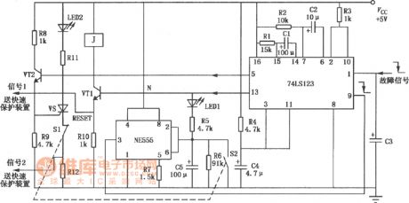
Most of the over-current, overvoltage protection of the power supply will stop working after the power failure, the output will be zero, and then it can be manually reset to work again; Or it only has temporary protection that will stop the power output after the failure happened. After the delay time, the power supply will automatically return to work. But in many devices, they require temporary protection and the die protection. For example, it requires the power to allow the load transient ignition and overcurrent. (View)
View full Circuit Diagram | Comments | Reading(660)
SIMPLE_JFET_PRESELECTOR
Published:2009/7/9 1:14:00 Author:May


This preselector will improve the performance of simple shortwave receivers. L2 is tuned with Q1.The inductance of L2 is:and L1is found around the cold end of L2. Typically, L1 has 10%of the turnsin L2, or one turn, which-everis larger. (View)
View full Circuit Diagram | Comments | Reading(903)
PHASE_SPLTTING_PREAMP
Published:2009/7/20 22:51:00 Author:Jessie

Uses Motorola MPSA13 operational integrator to provide 90° phase shift for MC1709 inverting opamp, with single-ended output complemented by phase splitting amplifier to provide push-pull drive for power amplifier of 115-V 60-Hz senvomotor, Voltage gain is about 40 dB.-A Pshaenich, Servo Motor Drive Amplifiers, Motorola, Phoenix,AZ,1972,AN-590. (View)
View full Circuit Diagram | Comments | Reading(1175)
903_MHz_LINEAR_AMPLIFIERS
Published:2009/7/9 1:12:00 Author:May


Two W output can be produced by this circuit designed for the 902- to 928-MHz amateur band. As shown in the figures, much of the circuitry is in the form of PC board traces. (View)
View full Circuit Diagram | Comments | Reading(651)
DOUBLE_TUNED_JFET_PRESELECTOR
Published:2009/7/9 1:10:00 Author:May


This circuit uses an MPF102 JFET and a double-tuned common-gate amplifier. Gain is typically 10 to 15 dB∶L1≈ 10% turns on L2 or 1 turn (larger of these two). (View)
View full Circuit Diagram | Comments | Reading(2502)
ULTRASONIC_PEST_CONTROLLER
Published:2009/7/9 1:10:00 Author:May
This circuit consists of two basic parts: an oscillator tuned to 40 kHz, and a voltage doubler with pulse generator. The pulses are about 10 ms long and occur 2 -3 per s to reduce battery drain and increase the annoyance factor for a cat, dog, hedgehog, etc. The voltage doubling action increases the available output power for any given battery voltage. (View)
View full Circuit Diagram | Comments | Reading(787)
Electronic_organ_master_oscillator_using_an_ECG1026_thin_film_hybrid_module
Published:2009/7/20 22:51:00 Author:Jessie

Electronic organ master oscillator using an ECG1026 thin-film hybrid module. Output is taken at pin 7, where the VTVM is shown connected to test output voltage level (courtesy GTE Sylvania Incorporated). (View)
View full Circuit Diagram | Comments | Reading(569)
ULTRASONIC-PULSED_PEST_CONTROLLER
Published:2009/7/9 1:07:00 Author:May

IC2 forms a stable oscillator whose frequency and pulse width is determined by the values of R4, R5, R6, and C4. R4 is made adjustable for precise frequency setting. The output of IC2 is pin 3, which is capacitively coupled to the base of Q1. L1 acts as a high-impedance choke to the signal, while allowing the collector of Q1 to be dc-biased. Q1 amplifies the positive pulses from IC2 and step drives the series resonant combination of L2 and TD1. Resistor R10 serves to broaden the response of this resonant circuit. L2 and the inherent capacity of the transducer, TD1, forms a resonant circuit at around 23 kHz. It is usually found that most rodents are bothered when the signal is pulsed with the off exceeding the on time. This timing is accomplished via timer IC1 and timer inverter Q2. IC1 is free running and its periods are determined by R1, R2, and C2 to be approximately two seconds off and two seconds on. The periods are inverted via Q2 and used to gate pin 4 of IC2, the frequency oscillator, tuming it on for two seconds and off for three seconds. The power supply is a conventional voltage doubler with a zener regulator for the oscillator voltages. (View)
View full Circuit Diagram | Comments | Reading(966)
10_MHz_oscillator_using_a_single_ECG703A_chip_that_can_be_used_as_a_short_range_transmitter
Published:2009/7/20 22:50:00 Author:Jessie

10 MHz oscillator using a single ECG703A chip that can be used as a short range transmitter. it is possible to modulate the oscillator by inserting the audio modulator shown between pin 1 and the tank circuit (courtesy GTE Sylvania Incorporated). (View)
View full Circuit Diagram | Comments | Reading(522)
Linear_amplitude_modulator_circuit_using_an_AD534_multiplier_divider_chip
Published:2009/7/20 22:50:00 Author:Jessie

Linear amplitude modulator circuit using an AD534 multiplier/divider chip(courtesy Analog Devices,Inc.). (View)
View full Circuit Diagram | Comments | Reading(2417)
10_to_15_W_ATV_LINEAR_AMPLIFIER
Published:2009/7/9 1:07:00 Author:May

This amplifier is useful for applications where a 10- to 15-W peak-envelope-power (PEP) signal is needed in the 420- to 520-MHz range. C1, C2, and L1 form a matching network for amplifter Q1. L3, C3, and C4 form an output matching network for a 50-Ω load. L2, R2, D1, and R3 through R6with bias adjust R1) form a biasing network for Q1. D2 and D3 provide polarity protection for Q1, which must be heat-sinked. A kit of all parts including case and PC board is available from North Country Radio, P.O. Box 53, Wykagyl Station, New Rochelle, NY 10804. (View)
View full Circuit Diagram | Comments | Reading(968)
Machine tool magnetic chuck undercurrent protection circuit diagram
Published:2011/8/2 2:43:00 Author:Rebekka | Keyword: Machine tool magnetic chuck , undercurrent protection
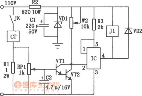
The signal from the sampling circuit is amplified by voltage, whichmakes the collector potential of VTl, VT2 close to 0V, the ② pin of IC's is at the low potential , ④ pin is turned on, relay J1 gets the power. The dynamic co-contact is closed, so that the machine starts to work. When the magnetic chuck current is less than 90% of rated current (this value is adjustable), IC's ④ pin is stopped. J1 is off, the machine feed-through circuit is off at the same time. The feed-though system stops working, thus avoids the accident. This circuit IC uses TWH8751 type, VTl uses 9013-type, VT2 uses 3DGl2 type, VDl uses 24V, 1W. VD2 uses lN4148 type, relay J1 uses JTX-24 type. (View)
View full Circuit Diagram | Comments | Reading(1637)
6_m_100_WILNEAR_AMPLIFIER
Published:2009/7/9 1:05:00 Author:May


100 W output at 50 MHz is available from this circuit. UI and Q2 form a T-R relay driver, switching the amplifier on when RF input at J1 is sensed. During receive periods, J1 and J2 are directly connected. A 13.8-V supply is required for this amplifier. (View)
View full Circuit Diagram | Comments | Reading(877)
105_MHz_gate_2_controlled_RF_amplifier_using_a_TIS152_dual_gate_MOSFET
Published:2009/7/20 22:46:00 Author:Jessie

105 MHz gate-2-controlled RF amplifier using a TIS152 dual-gate MOSFET (courtesy Texas Instruments Incorporated). (View)
View full Circuit Diagram | Comments | Reading(805)
SIDEBAND_RF_AMPLIFIER
Published:2009/7/9 1:02:00 Author:May

This RF amplifier has wide bandwidth and dynamic range. It has a gain of 10 dB, noise figure less than 5 dB, and the third-order 1 MD is -40 dB at +22 dBm/tone output. The bandwidth is 4 to 55 MHz. (View)
View full Circuit Diagram | Comments | Reading(795)
| Pages:918/2234 At 20901902903904905906907908909910911912913914915916917918919920Under 20 |
Circuit Categories
power supply circuit
Amplifier Circuit
Basic Circuit
LED and Light Circuit
Sensor Circuit
Signal Processing
Electrical Equipment Circuit
Control Circuit
Remote Control Circuit
A/D-D/A Converter Circuit
Audio Circuit
Measuring and Test Circuit
Communication Circuit
Computer-Related Circuit
555 Circuit
Automotive Circuit
Repairing Circuit