
Circuit Diagram
Index 903
MICROPHONE_PREAMP_
Published:2009/7/9 3:34:00 Author:May
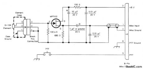
This circuitis used to interface a high-impedance microphone to a radio transceiver that requires alow-impedance microphone.The supply voltage can be either a battery or taken from the transceiver thecircuit is used with. (View)
View full Circuit Diagram | Comments | Reading(767)
50_W_OFF_LINE_SWITCHING_POWER_SUPPLY
Published:2009/7/9 3:33:00 Author:May
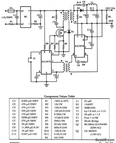
The schematic shows a 50-W power supply with a 5-V 10-A output. It is a flyback converter operating in the continuous mode. The circuit features a primary side and secondary side controller will full-protection from fault conditions such as overcurrent. After the fault condition has been removed, the power supply will enter the soft-start cycle before recommencing normal operation. (View)
View full Circuit Diagram | Comments | Reading(896)
LOW_COST_3_A_SWITCHING_REGULATOR
Published:2009/7/9 3:30:00 Author:May

View full Circuit Diagram | Comments | Reading(993)
FREQUENCY_VOLTAGE_CONVERTER
Published:2009/7/9 3:29:00 Author:May


A dc output that is proportional to frequency can be derived with this circuit. It is useful for analog frequency meter or tachometer applications. (View)
View full Circuit Diagram | Comments | Reading(2081)
SAFE_CONSTANT_CURRENT_SOURCE
Published:2009/7/9 3:28:00 Author:May
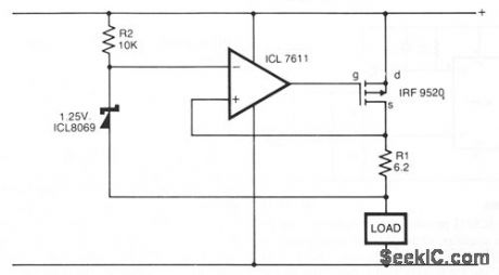
In the circuit shown, a CMOS op amp controls the current through a p-channel HEXFET power transistor to maintain a constant voltage across R1. The current is given by: 1 = VREF/R1. The advantages of this configuration are: (a) in the event of a component failure, the load current is limited by R1; and (b) the overhead voltage needed by the op amp and the HEXFET is extremely low. (View)
View full Circuit Diagram | Comments | Reading(1009)
LOW_IMPEDANCE_MICROPHONE_PREAMP
Published:2009/7/9 3:27:00 Author:May
This amplifter uses a common-gate FET amplifter to match a low-Z microphone. (View)
View full Circuit Diagram | Comments | Reading(963)
LOW_FORWARD_DROP_RECTIFIER_CIRCUIT
Published:2009/7/9 3:27:00 Author:May
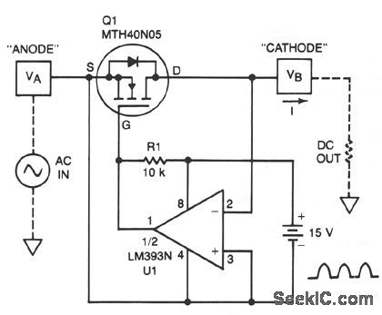
A TMOS power FET, Q1, and an LM393 comparator provide a high-efficiency rectifter circuit. When VA exceeds VB, U1's output becomes high and Q1 conducts. Conversely, when VB exceeds VA, the comparator output becomes low and Q1 does not conduct.The forward drop is determined by Q1's on resistance and current I. The MTH40N05 has an on resistance of 0.028 Ω; for I = 10 A, the forward drop is less than 0.3 V. Typically, the best Schottky diodes do not even begin conducting below a few hundred mV. (View)
View full Circuit Diagram | Comments | Reading(2211)
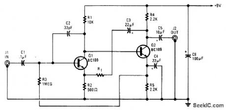
LOW_NOISE_AUDIO_PREAMP
Published:2009/7/9 3:26:00 Author:May
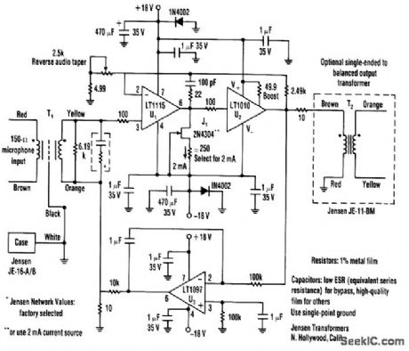
A low-noise LT1115 (Linear Technology, Inc.) op amp is coupled to class-A buffer amplirier to produce a variable gain (12-to-50 dB) microphone preamp. THD is less than 0.01% from 80Hz to over 20kHz. The transformers must be properly grounded and shielded. (View)
View full Circuit Diagram | Comments | Reading(2113)
COMPUTER_SPEECH_SYNTHESIZER
Published:2009/7/9 3:25:00 Author:May

This text-to-speech converter is built around the SPO256-AL2 speech processor and the CT6256-AL2 text-to-speech converter chips-manufactured by General Instruments. The circuit is set up to receive standard ASCII code from virtually any microcomputer or dumb terminal that is equipped with an RS-232 port-such as a serial-printer or modem port. If a microcomputer is used, the synthesizer can be activated from a terminal-emulator of any communications proaram, or front any programming language such as BASIC.The serial input from the RS-232 port enters the circuit through U7, the MC1489 RS-232 receiver chip, and is converted from an RS-232 level to a TTL-level signal. The CTS256-AL2 chip, U1, then converts the ASCII characters into allophone codes and sends those codes to U3, the TMS4016 external-RAM chip. The codes are then transferred to the SPO256-AL2, U2, through the 74LS373 octal latch, U4. Finally, the SPO256-AL2 sends out an audio signal to the LM386 audio amplifier, U8, through some highpass filtering, and on to the speaker. The 74LS138d, US, and the 74LSO4, U6, provide control logic. (View)
View full Circuit Diagram | Comments | Reading(3131)
FREQUENCY_VOLTAGE_CONVERTER_WITH_SAMPLE_AND_HOLD
Published:2009/7/9 3:25:00 Author:May

U1 is a frequency/voltage converter, feeding sample-and-hold circuit using an LF381. An LF351 pro-vides 10-V full-scale output. The circuit produces 1-V/kHz output. (View)
View full Circuit Diagram | Comments | Reading(694)
POSITIVE_REGULATOR_WITH_PNP_BOOST
Published:2009/7/9 3:23:00 Author:May


The IC8211 provides the voltage reference and regulator amplifier, while Q1 is the series pass transistor. R1 defines the output current of the IC8211, while C1 and C2 provide loop stability and also act to suppress feedthrough of input transients to the output supply. R2 and R3 determine the output voltage as follows:output supply. R2 and R3 determine the output voltage as follows:In addition, the values of R2 and R3 are chosen to provide a small amount of standing current in Q1, which gives additional stability margin to the circuit.Where accurate setting of the output voltage is required, either R2 or R3 can be made adjustable. If R2 is made adjustable, the output voltage will vary linearly with the shaft angle; however, if the potentiometer wiper was to open the circuit, the output voltage would rise. In general, therefore, it is better to make R3 adjustable, since this gives fail-safe operation. (View)
View full Circuit Diagram | Comments | Reading(1377)
FREQUENCY_VOLTAGE_CONVERTER_WITH_OPTOCOUPLER_INPUT
Published:2009/7/9 3:21:00 Author:May

In this circuit, the input from IC2 optocoupler is fed to the comparator input of the AD650 (Analog Devices or Maxim Electronics) V/F converter. This internally generates a pulse that is fed to the op amp, which outputs a dc voltage that is proportional to frequency. Component values are shown in the figure. (View)
View full Circuit Diagram | Comments | Reading(876)
DIALED_PHONE_NUMBER_VOCALIZER
Published:2009/7/9 3:21:00 Author:May

By vocalizing the numbers and symbols of its keypad, the phone provides an audible confirmation that is useful to the blind. The serial-interface, 2 K-byte x 8-bit ROM (IC4) stores programmed sequences of instructions that are executed by the speech-processor chip IC2-manufactured by the General Instrument Corp. When you depress a key, tone-dialing chip IC1 issues the corresponding number of pulses at its DP output. Counter IC5 totals the pulses, and IC6 latches the resulting 4-bit digital word. This word, converted to serial format by IC2, becomes an address that selects a block of memory within IC4. (View)
View full Circuit Diagram | Comments | Reading(931)
CD4O49_AMPLIFIER
Published:2009/7/9 3:20:00 Author:May

When an inverter is biased with one resistor from its input to output in the range of 100 kΩ to 10 MΩ and is capacitor coupled, it exhibits amplifier characteristics (see the table).
Furthermore, when a split power-supply bus is needed and only one battery is used, the inverter can be configured to supply a pseudo-dc ground of relatively low impedance, coincident with the ac ground (see the ftgure). Depending on the magnitude of the dc ground return currents, anywhere from one inverter to several in parallel are sufficient. Also, the supply buses must be capacitor bypassed.
The configured inpqt-to-input shorted inverter now acts as a voltage regulator that sinks and sources current. In this configuration, the inverter is forced to operate at the midpoint of its transfer characteristic. This divides the battery potential into two equal parts-as referenced to the defined dc ground by virtue of its internal gain and physical structure. Op amps such as the LM324A, can be powered from one battery while being referenced to the dc ground that is generated by the inverter. This novel technique surpasses the use of discrete resistors for battery potential dividing. It can be employed in other applications where individual component savings and improved design performance are needed. (View)
View full Circuit Diagram | Comments | Reading(667)
POWER_CONVERTER
Published:2009/7/9 3:20:00 Author:May
This circuit consists of an astable multivibrator driving a push-pull pair of transistors into the trans-former primary. The multivibrator frequency should equal around 1 or 2 kHz. For higher dc voltages, voltage multipliers on the secondary circuit have been used successfully to generate 10 kV from a 40-stage multiplier like the one shown. (View)
View full Circuit Diagram | Comments | Reading(1)
BILATERAL_CURRENT_SOURCE
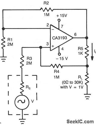
Published:2009/7/9 3:19:00 Author:May


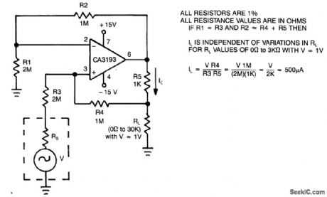
This circuit uses a CA3193 precision op amp to deliver a current independent of variations in RL. With A1 set equal to R3, and R2 approximately equal to R4 + R5, the output current, IL is:VIN (R4)/(R3) (R5). 500-μA load current is constant for load values from 0 to 3 Ω. (View)
View full Circuit Diagram | Comments | Reading(0)
WATER_LEVEL_MEASUREMENT_CIRCUIT
Published:2009/7/9 3:18:00 Author:May


Using a capacttor sensor to detect a water level is a simple method of sensmg.This circuit uses C5,which is 10 to 20 of ﹟22 enamelled wlre as one electrode,This shifts the oscillator, an NE556 timer, infrequency..The frequency shift depends on the capacitance charge,which In turn vanes with water level.Ameter connected to pin 9 of the 556 is used as an indicator. C5 can be made larger or smaller to suit the intended application. (View)
View full Circuit Diagram | Comments | Reading(2745)
UNIVERSAL_AUDIO_LINE_AMPLIFIER
Published:2009/7/9 3:17:00 Author:May
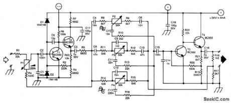
A line amplifier is always a useful unit to have around, whether it is for matching a line signal or raising its level somewhat. This might be needed during a recording session or with a public-address system. Furthermore, a line mixer can be constructed from a number of these amplifiers. The input of the amplifier is high-voltage proof. The output impedance is low.
The circuit is a conventional design: two dc-coupled stages of amplification are separated by a three-fold Baxandall tone control system. The volume control at the input is conspicuous by having its cold side connected, not to ground, but to the output of the first amplifier. Because the signal there is out of phase with the input signal, the amplifier obtains negative feedback via P1. The amplification is therefore inversely proportional to the magnitude of the input signal. Thus, it is possible for the amplifier to accept a wide range of input levels. It is quite possible to input a signal taken directly from the loudspeaker termi-nals of a power amplifier.
The supply voltage is 24 V. At that voltage, the amplifier draws a current of about 4 mA. If several amplifiers are used in conjunction (as, for instance, in a mixer panel), the various supplies (+ and ++ in the diagram) can be interlinked. Capacitors C17 and C18, and resistor R7 don't need to be duplicated in that case. (View)
View full Circuit Diagram | Comments | Reading(3608)
CHARGE_POOL_POWER_SUPPLY
Published:2009/7/9 3:17:00 Author:May


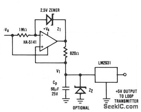
It is usually desirable to have the remote transmitter of a 4 to 20 mA current loop system powered directly from the transmission line. In some cases, this is not possible because of the high-power requirements set by the remote sensor/transmitter system. In these cases, an alternative to the separate power supply is still possible. If the remote transmitter can be operated in a pulsed mode where it is active only long enough to perform its function, then a charge pool power supply can still allow the transmitter to be powered directly by the current loop. In this circuit, constant current I1 is supplied to the charge pool capacitor, CP, by the HA-5141 (where I1 = 3 mA). The voltage V1 continues to rise until the output of the HA-5141 approaches + VS or the optional voltage limiting prodded by Z2. The LM2931 voltage regulator supplies the transmitter with a stable +5 V supply from the charge collected by CP. Available power supply current is determined by the duration, allowable voltage droop on CP, and required repetition rate. For example, if F1 is allowed to droop 4.4 V and the duration of operation is 1 ms, the available power supply current is approximately: (View)
View full Circuit Diagram | Comments | Reading(620)
AC_LINE_VOLTAGE_ANNOUNCER
Published:2009/7/9 3:16:00 Author:May

The range of this ac-voltage monitor is 100 to 140 Vac, with a resolution of 1 V. The speech processor interprets an 8-bit binary input code from an analog-to-digital converter. The processor's pulse-code-modulated output then passes through a filter and an amplifier before driving the circuit's speaker to vocalize the corresponding number. Each time switch S1 is pressed, the speech-processor program enunciates the monitored voltage readings from 100 to 140 V, depending on the code at the input of a 27C64 EPROM.The voltage-monitoring circuit consists of a bridge rectifier, filter capacitors, and a 10-KΩ load resistor. A divider, RA and RB, limits the input voltage to a maximum 2.55 V. The a/d converter, IC4, then sends the voltage reading to the 27C64 EPROM, ICS. Pressing S1 sends a negative transient pulse to the write, WR, input of the a/d converter, IC4, which initiates a 100-μs conversion process. (View)
View full Circuit Diagram | Comments | Reading(1736)
| Pages:903/2234 At 20901902903904905906907908909910911912913914915916917918919920Under 20 |
Circuit Categories
power supply circuit
Amplifier Circuit
Basic Circuit
LED and Light Circuit
Sensor Circuit
Signal Processing
Electrical Equipment Circuit
Control Circuit
Remote Control Circuit
A/D-D/A Converter Circuit
Audio Circuit
Measuring and Test Circuit
Communication Circuit
Computer-Related Circuit
555 Circuit
Automotive Circuit
Repairing Circuit