
Circuit Diagram
Index 912
Home booster pump protection circuit diagram
Published:2011/8/2 2:37:00 Author:Rebekka | Keyword: Home booster pump protection
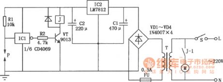
The power supply switch S will be closed if the water pipe has not water, P and the ground is similar to insulation condition, the inverter ICl inputs high, outputs low, VT cuts off, J is released. Its tragger J-1 cuts off, M booster pump is not running avoiding pump idling. If the pipe has water, P and steel shell pass the water and resistance will be conducted, then ICl input is low level and output is high level, VT will be conducted, J pulls in, M operates normally. IC1 uses CD4069 six-inverter, the one shown in the figure only uses one group of inverters, and the rest 5 groups of inverters is vacant(Connect all the input ends to the ground to prevent interference.) P is the detection sensor when there is not water, you need to make it by yourself. Methods: Drill a hole in the pipe, spark plugs into the car, pay attention to the pad to prevent leakage, eads to P pole at the spark needle, water pipe(steel) chassis can connect to the ground. (View)
View full Circuit Diagram | Comments | Reading(1187)
SEQUENTIAL_FLASHER
Published:2009/7/9 2:00:00 Author:May

Using a 555 timer to drive a CMOS counter, this device uses RCA CA3079 zero-voltage switch to control triacs TRI through TR4. This circuit can be used to sequence lamp displays, etc.
Caution: The CA3079s are connected to the 117-V line, as is the clock and counter circuit and their power supplies. Use caution, good insulation, and safe construction practices. (View)
View full Circuit Diagram | Comments | Reading(0)
MARK_SENSOR_FOR_CARDS
Published:2009/7/20 10:23:00 Author:Jessie

Automatically transcribes up to 40 pencil marks on specially printed 90-column cards into machine code and block-punches information into cards in any desired format at 150 cards per minute -F. A. Frankl, Transcribing Field Markings by Optical Scanning, Electronics, 34:31, p 49-51. (View)
View full Circuit Diagram | Comments | Reading(1525)
SCOPE_SENSITIVITYAMPLIFIER
Published:2009/7/9 1:59:00 Author:May

This circuit provides 20 ±0.1 dB voltage gain from 0.5 to 25 MHz and ±3 dB from 70 kHz to 55 MHz. An LM733 video amplifter furnishes a low input-noise spec, 10-μV typical, measured over a 15.7-MHz bandwidth. The scale factor of the instrument can be preserved by using a trimmer R1 or a selected precision resistor, to set the circuit's voltage gain to exactly 100. (View)
View full Circuit Diagram | Comments | Reading(2911)
OSCILLOSCOPE_CALIBRATOR
Published:2009/7/9 1:59:00 Author:May

The calibrator can be used to check the accuracy of a time-base generator, as well as to calibrate the input level of amplifiers. The calibrator consists of an NE555 connected in the astable mode. The oscillator is set to exactly 1 kHz by adjusting potentiometer P1 while the output at pin 3 is being monitored against a known frequency standard or frequency counter. The output level, likewise, is monitored from potentiometer P2's center arm to ground with a standard instrument. P2 is adjusted for 1 V pk-pk at the calibrator output terminal. During operation, the calibrator output terminal will produce a 1-kHz, square-wave signal at 1 V pk-pk with about 50% duty cycle. For long-term oscillator frequency stability, C1 should be a low-leakage mylar capacitor. (View)
View full Circuit Diagram | Comments | Reading(878)
LAMP_PREHEATER
Published:2009/7/20 10:11:00 Author:Jessie

Unijunction transistor triggers LASCR (light-activated scr) late in each half-cycle, with R2 determining lamp current so filament is heated but not visible. This preheating minimizes thermal stresses during programmed operation of lamps by control beam hitting LASCR, as for theaters or fountains.-E. K. Howell, Light-Activated Switch Expands Uses of Silicon-Controlled Rectifiers, Electronics, 37:15, p 53-61. (View)
View full Circuit Diagram | Comments | Reading(1326)
NOISE_SUPPRESSOR
Published:2009/7/20 10:10:00 Author:Jessie

Removes noise from output of photodiode used in reflected-light shaft-position encoder. -F. W. Kear, How to Select Shaft-Position Encoders, Electronics, 35:35, p 48-51. (View)
View full Circuit Diagram | Comments | Reading(1904)
OUTPUT_STAGE_POWER_BOOSTER
Published:2009/7/9 1:58:00 Author:May

This circuit easily supplements the current-sourcing and current-sinking capability of the CA3130 BiMOS op amp. This arrangement boosts the current-handling capability of the CA3130 output stage by about 2.5 times. (View)
View full Circuit Diagram | Comments | Reading(1021)
200_MHz_RF_post_amplifier_usmg_two_3N204_dual_gate_MOSFETs
Published:2009/7/20 8:46:00 Author:Jessie

200 MHz RF post amplifier usmg two 3N204 dual-gate MOSFETs (courtesy Texas Instruments Incorporated). (View)
View full Circuit Diagram | Comments | Reading(730)
PRECISION_HQLF_WAVE_RECTIFIER
Published:2009/7/9 1:58:00 Author:May

An ac input voltage will cause an output that is a half-wave rectifted version of the input voltage.
(View)
View full Circuit Diagram | Comments | Reading(642)
50_W_AUDIO_POWER_AMPLIFIER
Published:2009/7/9 1:57:00 Author:May

This audio amplifier design approach employs TMOS Power FETs operating in a complementary common-source configuration. They are biased to cutoff, then turn on very quickly when a signal is applied.The advantage of this approach is that the output stage is very stable from a thermal point of view.U1 is a high slew-rate amp that drives Q3, Q4,and Q6 (operating class AB) providing level transition for the output stage consisting of Q7, Q8, Q9,and Q10. The positive temperature coefficient of the TMOS device enables parallel operation of Q7, Q8, and Q9 and provides a higher power complementary device for Q10. These TMOS Power FETs must be driven from a low-source impedance of 1000, in order to actually obtain high turn-on speeds. (View)
View full Circuit Diagram | Comments | Reading(801)
A_C_MODULATOR_FOR_PHOTOMULTIPLIER
Published:2009/7/20 8:03:00 Author:Jessie

Output of star-tracking photomultiplier is converted to a-c by applying 400-cps modulating voltage to dynode 14, to make gain vary between nominal value and 1% of this in square wave fashion. Amplifier passband is then 130 to 800 cps.-E. R. Schlesinger, Aiming a 3-Ton Telescope Hanging from Balloon, Electronics, 36:6, p 47-51. (View)
View full Circuit Diagram | Comments | Reading(860)
AUTOMATIC_CALIPER
Published:2009/7/20 7:58:00 Author:Jessie

Photomultiplier and counter circuit on machine lathe feed recorder to give dimensions of printed circuits and photographic plates in increments of 0.0001 inch.-S. Isaacson, Electronic Caliper Checks Printed Circuits, Electronics, 32:1, p 44-45. (View)
View full Circuit Diagram | Comments | Reading(634)
_EIGHT_OHANNEL_VOLTAGE_DISPLAY
Published:2009/7/9 1:57:00 Author:May

This circuit turns a common oscilloscope into a versatile eight-channel display for direct voltages. The trend of each of the eight input levels is readily observed, albeit that the attainable resolution is not very high.
The circuit diagram shows the use of an eight-channel analog multiplexer IC1, which is the electronic version of an eight-way rotary switch with contacts X0 through X7 and pole Y. The relevant channel is selected by applying a binary code to the A-B-C inputs. For example, binary code 011 (A-B-C) enables channel 7 ( X6 Y ). The A-B-C inputs of IC1 are driven from three successive outputs of binary counter IC2, which is set to oscillate at about 50 kHz with the aid of P1. Since the counter is not reset, the binary state of outputs Q5, Q6, and Q7 steps from 0 to 7 in a cyclic manner. Each of the direct voltages at input terminals 1 to 8 is therefore briefly connected to the Y input of the oscilloscope. All eight input levels can be seen simultaneously by setting the timebase of the scope, in accordance with the time it takes the counter to output states 0 through 7, on outputs Q5, Q6, and Q7.
The timebase on the scope should be set to 0.5 ms/div, and triggering should occur on the positive edge of the external signal. Set the vertical sensitivity to 1 V/div. The input range of this circuit is from -4 V to +4 V; connected channels are terminated in about 100 KΩ. (View)
View full Circuit Diagram | Comments | Reading(1093)
CORONAMETER
Published:2009/7/20 7:48:00 Author:Jessie


Uses polarized-light technique and closely controlled narrowband circuit to detect, observe, and measure otherwise invisible solar phenomenon. Circuit shows multiplier tube in optical head, with dynode supply, electro-optical light modulator (EOLM) driver amplifiers, polarization signal amplifier, and synchronous detector.-R. H. Lee and J. G. Fullerton, K-Coronameter Observes the Sun's Electron Corona, Electronics, 34:47, p 58-62. (View)
View full Circuit Diagram | Comments | Reading(1279)
RGB_COMPOSITE_CONVERTER
Published:2009/7/9 1:56:00 Author:May

The incoming RGB inputs are terminated with resistors R1, R2, and R3 and potentiometers RV1, RV2, and RV3. These provide input impedances of approximately 750. The presets should be adjusted to provide a maximum input of 1 V pk-pk into the MC1377. The inputs are ac-coupled into the encoder; the large value capacitor is required for the 60 Hz field component.The Colpitts oscillator for the color burst is formed around pins 17 and 18. About 0.5 V pk-pk should appear on pin 17 and 0.25 V rms into pin 18 with the oscillator components removed. The incoming composite sync signal at pin 2 should be negative-going. The device will accept CMOS and TTL directly. If it is necessary to ac-couple the sync, then a pull-up to 8.2 V is required-a regulated 8.2 V is provided on pin 16.From the composite sync input, the MC1377 generates a ramp which it uses to provide the burst gate pulse. The slope of this ramp can be varied by a potentiometer on pin 1. However, a preset value, shown as 43 KΩ, is usually sufficient. The chrominance filter should be fitted between pins 13 and 10. If the filter is not used, a compensatory potential divider should be fitted (both are shown). We used a prealigned Toko bandpass filter centered on 4.43 MHz. If the chroma filter is fitted, the delay through it, 400 ns, has to be compensated for by a luminance delay line between pins 6 and 8. This line is shorted out if the filter is not fitted. The composite video output from the IC is buffered to provide a low-impedance drive for a monitor, or it can be applied directly to a UHF modulator commonly used in computers. (View)
View full Circuit Diagram | Comments | Reading(1858)
VOICE_SCRAMBLER_DESCRAMBLER
Published:2009/7/9 1:55:00 Author:May

This circuit uses an NE602 as an inversion mixer. U2 is set to run at about 2.5 to 3.5 kHz. U3 drives a loudspeaker. Because speech inversion scrambling is its own inverse, the circuit will also descramble. (View)
View full Circuit Diagram | Comments | Reading(2306)
STROBE_ALARM
Published:2009/7/9 1:55:00 Author:May
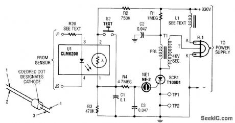
This strobe gives a visual indication of a sensor input. The input signal causes U1, a light dependent resistor, to charge C1 and C3 through R4. When NE1 fires, C3 discharges into SCR1, which triggers it and causes C2 to discharge through trigger transformer T1, which triggers Flashlamp FL1. The 330-V supply should have about 50 to 100 μF output capacitance. L1 supplies about 25-mH inductance to prolong the flash and the life of FL1. (View)
View full Circuit Diagram | Comments | Reading(1257)
ELECTRONIC_PHOTOFLASH
Published:2009/7/9 1:55:00 Author:May

Using the CA3164A BiMOS control chip consumes less than 15 μA during standby, yet it can provide 100 mA of chopped current to the dc-to-dc converter during the energy-reservoir charging cycle. The CA3164A drives the primary of T1 with symmetrically chopped current at a 400 to 2000 Hz rate. The CA3164A's chopper frequency is about 500 Hz; the duty cycle, 50% when R7 is 3.1 4 KΩ. (View)
View full Circuit Diagram | Comments | Reading(630)
SCR_FIRING_ANGLE_CONTROL
Published:2009/7/20 7:43:00 Author:Jessie
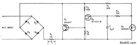
Unijunction transistor trigger circuit fires scr at specific time in each half-cycle of keep average load voltage constant over line voltage range of l00 to 200 v a-c.-R. S. Krochmal and W. Weber, Controling SCR Firing Angle Regulates D-C Load Voltage, Electronics, 38:16, p 80-81. (View)
View full Circuit Diagram | Comments | Reading(2465)
| Pages:912/2234 At 20901902903904905906907908909910911912913914915916917918919920Under 20 |
Circuit Categories
power supply circuit
Amplifier Circuit
Basic Circuit
LED and Light Circuit
Sensor Circuit
Signal Processing
Electrical Equipment Circuit
Control Circuit
Remote Control Circuit
A/D-D/A Converter Circuit
Audio Circuit
Measuring and Test Circuit
Communication Circuit
Computer-Related Circuit
555 Circuit
Automotive Circuit
Repairing Circuit