
Circuit Diagram
Index 915
1000_1_TUNING_VOLTAGE_VOLTAGE_CONTROLLED_FILTER
Published:2009/7/9 1:39:00 Author:May

A standard dual integrator ftlter can be constructed using a few CA3080s. By varying IABC, the reso-nant frequency can be swept over a 1000:1 range. At IC1, three are current-controlled integrators. At IC2, four are voltage followers that serve to buffer the high-impedance outputs of the integrators. A third CA3080 (IC5) is used to control the Q factor of the filter. The resonant frequency of the ftlter is linearly proportional to IABC. Hence, this unit is very useful in producing electronic music. Two outputs are pro-duced: a low-pass and a bandpass response. (View)
View full Circuit Diagram | Comments | Reading(827)
AUDIO_OSCILLATOR
Published:2009/7/9 1:38:00 Author:May

The circuit's frequency of oscillation is f = 2.8/[C1×(R1+ R2)]. Using the values shown, the output frequency can be varied from 60 Hz to 20 kHz by rotating potentiometer R2.
A portion of IC1's output voltage is fed to its noninverting input at pin 3. The voltage serves as a reference for capacitor C1, which is connected to the noninverting input at pin 2 of the IC. That capacitor continually charges and discharges around the reference voltage, and the result is a square-wave output. Capacitor g2 decouples the output.
(View)
View full Circuit Diagram | Comments | Reading(0)
TRANSFORMERLESS_COLLECTOR_MODULATOR
Published:2009/7/21 0:11:00 Author:Jessie

Provides 950 mw modulated power for CB transmitter, but 100% modulation can be reached only by using double modulation.-B. Rheinfelder, Modulation Techniques for Transistorized A-M Transmitters, EEE, 11:7, p 54-57. (View)
View full Circuit Diagram | Comments | Reading(700)
MUSICAL_ENVELOPE_GENERATOR_AND_MODULATOR
Published:2009/7/9 1:38:00 Author:May

A gate voltage is applied to initiate the proceedings. When the gate voltage is in the ON state, Q1 is turned on, and capacitor C is charged up via the attack pot in series with the 1-kΩ resistor. By varying this pot, the attack time'constant can be manipulated. A fast attack gives a percussive sound, a slow attack gives the effect of backward sounds. When the gate voltage returns to its OFF state, Q2 is turned on and the capacitor is then discharged via the decay pot and the other 1-kΩ resistor to ground. Thus, the decay time constant of the envelope is also variable.
This envelope is buffered by IC1, a high-impedance voltage follower and is applied to Q3, which is being used as a transistor chopper. A musical tone in the form of a square wave is connected to the base of Q3. This turns the transistor on or off, Thus, the envelope is chopped up at regular intervals, which are determined by the pitch of the square wave.
The resultant waveform has the amplitude of the envelope and the harmonic structure of the square wave. IC2 is used as a virtual earth amplifier to buffer the signal and Dl ensures that the envelope dies away at the end of a note. (View)
View full Circuit Diagram | Comments | Reading(1618)
Anbaolu microwave safe control board circuit diagram
Published:2011/8/2 2:23:00 Author:Rebekka | Keyword: Anbaolu, microwave safe control board
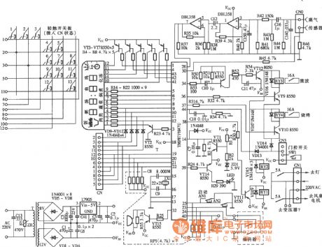
Here is the diagram of anpo road microwave safe control board circuit. (View)
View full Circuit Diagram | Comments | Reading(2160)
415_MHz_frequency_modulated_oscillator_using_a_3N204_dual_gate_MOSFET
Published:2009/7/20 23:38:00 Author:Jessie

415 MHz frequency-modulated oscillator using a 3N204 dual-gate MOSFET. The 3N212 must be selected for IDSS greater than 20 mA (courtesy Texas Instruments Incorporated). (View)
View full Circuit Diagram | Comments | Reading(683)
CAMERA_ALARM_TRIGGER
Published:2009/7/9 1:36:00 Author:May

Transistor Q1 remains off until the magnetic switch connected to J1 closes. When that happens, the 9 V is connected through R1 to Q1'S base. Q1 turns on, thereby charging C2 through relay K1, which causes K1's contacts to close. Since the contacts connect via J2 to the remote control jack in the camera, which in turn connects to the camera's shutter release, the closure of K1's contacts will cause the camera's shutter to trigger. After C2 charges, K1 opens because current through its coil ceases; the camera won't take another picture. If Q1 turns off because the magnetic switch on the window or gate opens, C2 discharges and the circuit is ready for another cycle. As long as Q1 remains on, C2 stays charged and prevents K1 from triggering more photos. Capacitor C1 bypasses spurious magnetic switch noises from physical phenomena, such as a rattling window or a gate shaking in the wind, thus reducing the likelihood of an unwanted picture. Resistor R2 biases Q1 and dampens K1/C2 oscillations which might cause contact bounce. Diode D1 prevents C2 from discharging through K1; the relay coil isn't polarity conscious and C2 discharging through it would trigger an unwanted picture. (View)
View full Circuit Diagram | Comments | Reading(673)
PAM_MODULATOR_DECOMMUTATOR_FOR__VIDEO_RECORDER
Published:2009/7/20 23:39:00 Author:Jessie

Schmitt trigger reshapes timing pulses from 52-channel distributing delay line. Modulator samples audio signal from one channel during record mode, while decommutator separates individual channels from composite signal during playback from time-division multiplexing on two-track video recorder.-M. H. Damon and F. J. Messina, High-Density Storage of Wideband Analog Data, Electronics, 35:13, p 45-49. (View)
View full Circuit Diagram | Comments | Reading(969)
Voltage_controlled_oscillator
Published:2009/7/20 23:40:00 Author:Jessie

Voltage-controlled oscillator. This three-section phase-shift oscillator produces a good sine wave that is linear over the range indicated (courtesy Motorola Semiconductor Products Inc.). (View)
View full Circuit Diagram | Comments | Reading(0)
PULSE_FORMING_MODULATOR_FOR_LASERFLASH_LAMP
Published:2009/7/20 23:41:00 Author:Jessie

Saturating-core trigger transformer T1 responds to short high-voltage spike on leading edge of main pulse, generated by discharge of C2 through ceramic hydrogen thyratron switch tube when this tube is triggered on its grid.-S. J. Grabow- ski, Pulse Power Supply Design for Laser Pumping, Electronics, 36:51, p 33-35. (View)
View full Circuit Diagram | Comments | Reading(719)
20_watt_55_dB_16_to_30_MHz_SSB_linear_amplifier_for_mobile_operation
Published:2009/7/20 23:41:00 Author:Jessie


20-watt 55 dB 1.6 to 30 MHz SSB linear amplifier for mobile operation (courtesy Motorola Semiconductor Products Inc.).
(View)
View full Circuit Diagram | Comments | Reading(911)
BALANCED_MODULATOR_FOR_ADF
Published:2009/7/20 23:41:00 Author:Jessie
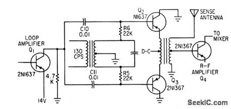
Combines signals from loop and sense antennas of automatic direction finder, to give 130-cps output having correct phase for driving rotor of resolver to null position.-P. V.Sparks, Servo Filter and Gain Control lmprove Automatic Direction Finder, Electronics, 34:23, p 110-113. (View)
View full Circuit Diagram | Comments | Reading(2034)
FOUR_CHANNEL_PPM_MODEM
Published:2009/7/20 23:42:00 Author:Jessie

Amplitude modulation of microwave radio system is pulse-position. modulated by multiplexor. Modulator-demodulator circuit handles 300 to 3,500-cps voice signals with amplitudes from -20 to +10 dbm.-P. W. Kiesling, Jr., Portable multiplexor for Telephone Communications, Electronics, 32:2, p 60-62. (View)
View full Circuit Diagram | Comments | Reading(1087)
VCO_and_mixer_for_CB_operation_using_a_single_3N204_dual_gate_MOSFET
Published:2009/7/20 23:43:00 Author:Jessie

VCO and mixer for CB operation using a single 3N204 dual-gate MOSFET (courtesy Texas Instruments Incorporated). (View)
View full Circuit Diagram | Comments | Reading(653)
9V 55mA AC and DC converter circuit composed of TNY253P
Published:2011/8/3 2:39:00 Author:Rebekka | Keyword: 9V , 55mA , AC and DC , converter
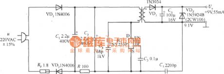
9V 55mA AC and DC converter circuit composed of TNY253P is shown as above. It can enable the end (EN) hang in air to simplify the circuit, TNY253P operates in the continuous conducting mode and outputs constant power. The output voltage is set by the regulator VDz. (View)
View full Circuit Diagram | Comments | Reading(682)
LAST_CYCLE_COMPLETING_GATED_OSCILLATOR
Published:2009/7/9 1:36:00 Author:May

Regenerative feedback at C enables the oscillator to complete its timing cycle, rather than immediately shutting it off. The IC used was a CD4011AE, although an equivalent will work. (View)
View full Circuit Diagram | Comments | Reading(885)
Voltage_controlled_crystal_oscillator
Published:2009/7/20 23:43:00 Author:Jessie

Voltage-controlled crystal oscillator. Operating range is 1 MHz to 20 MHz depending on the selected crystal and tank tuning. Tunign range is from zero to 25 volts. It is possible to make the tuning range from zero to -25 volts by reversing the varactor (courtesy Motorola Semiconductor Products Inc.). (View)
View full Circuit Diagram | Comments | Reading(0)
SIMPLE_RUMBLE_FILTER
Published:2009/7/9 1:35:00 Author:May

This circuit is a two-section active HP filter using an LM387, with a cutoff below 50 Hz at 12-dB per octave. It will help reduce rumble as a result of turntable defects in record systems. (View)
View full Circuit Diagram | Comments | Reading(854)
ANALOG_DELAY_LINEECHO_AND_REVERB
Published:2009/7/9 1:35:00 Author:May

This circuit uses an SAD 512D (Reticon) chip, which is a 512-stage analog shift register. By varying the clock frequency between 5 and 50 kHz, delay time can be set between 51.2 and 5.12 ms. The clock fre-quency must be at least twice the highest audio frequency. (View)
View full Circuit Diagram | Comments | Reading(1702)
PULSE_WIDTH_FREQUENCY_MODULATION
Published:2009/7/20 23:37:00 Author:Jessie

Gives pulse ratio modukttion, in which pulse duty ratio varies linearly with input signal.Accuracy is high over wide dynamic range.Developed for space vehicle control.-R. A.Schaefer, New Pulse Modulation Method Varies both Frequency and Width, Electronics, 35:41, p 50-53. (View)
View full Circuit Diagram | Comments | Reading(984)
| Pages:915/2234 At 20901902903904905906907908909910911912913914915916917918919920Under 20 |
Circuit Categories
power supply circuit
Amplifier Circuit
Basic Circuit
LED and Light Circuit
Sensor Circuit
Signal Processing
Electrical Equipment Circuit
Control Circuit
Remote Control Circuit
A/D-D/A Converter Circuit
Audio Circuit
Measuring and Test Circuit
Communication Circuit
Computer-Related Circuit
555 Circuit
Automotive Circuit
Repairing Circuit