
Circuit Diagram
Index 914
Positive_voltage_regulators_for_5_6_12_15_or_24_volts_using_the_ECG9XX_series
Published:2009/7/20 20:44:00 Author:Jessie
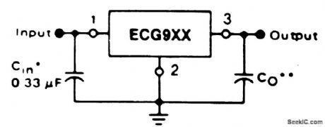
Positive voltage regulators for 5, 6, 12, 15, or 24 volts using the ECG9XX series.Rating for the three-terminal ECG9XX positive voltage regulators are as follows: ECG960, 5 volts; ECG962, 6 volts; ECG966, 12 volts; ECG968, 15 volts; and ECG972, 24 volts. A common ground is required between the input and output voltages. The input voltage must remain typically 2 volts above the output voltage even during the low point on the ripple (courtesy GTE Sylvania Incorporated). (View)
View full Circuit Diagram | Comments | Reading(594)
LINEAR_SCALE_OHMMETER_1
Published:2009/7/20 20:44:00 Author:Jessie

Provides accurate measurements of resistance in four ranges,with linear scale at high end of each.-Circuits,73 Magazine.Feb 1977,p27. (View)
View full Circuit Diagram | Comments | Reading(1740)
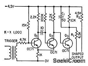
SLAVE_PHOTOGRAPHIC_XENON_FLASH_TRIGGER
Published:2009/7/9 1:48:00 Author:May


This circuit is used for remote photographic flash units that flash at the same time as the flash attached to the camera. This circuit is designed to the trigger cord or hot shoe connection of a commercial portable flash unit and triggers the unit from the light produced by the light of the flash unit attached to the camera. This provides remote operation without the need for wires or cables between the various units. The flash trigger unit should be connected to the slave flash before turning the flash on to prevent a dV/dt triggered flash on connection. The L14C1 phototransistor has a wide, almost cosine viewing angle, so alignment is not critical. If a very sensitive, more directional remote trigger unit is desired, the circuit can be modified using an L14G2 lensed phototransistor as the sensor.The lens on this transistor provides a viewing angle of approximately 10° and gives over a 10 to 1 improvement in light sensitivity (3 to 1 range improvement). Note that the phototransistor is connected in a self-biasing circuit which is relatively insensitive to slow-changing ambient light, and yet discharges the 0.01-μF capacitor into the C106D gate when illuminated by a photo flash. For a physically smaller size, the C106D can be replaced by a C205D, if the duty cycle is reduced appropriately. (View)
View full Circuit Diagram | Comments | Reading(1080)
CMOS_OSCILLATOR_1
Published:2009/7/9 1:48:00 Author:May


The common clock oscillator in Fig. 68-19A has two small problems: It might not, in fact, oscil-late if the transition regions of its two gates differ. If it does oscillate, it might sometimes oscillate at a slightly lower frequency than its equation predicts because of the fmite gain of the ftrst gate. If the circuit does work, oscillation occurs usually because both gates are in the package and, therefore, have logic thresholds only a few millivolts apart.
The circuit in Fig. 68-19B resolves both prob-lems by adding a resistor and a capacitor. The R2/ C2 network provides hysteresis, thus delaying the onset of gate 1's transition until C1 has enough voltage to move gate 1 securely through its transi-tion region. When gate 1 is finally in its transition region, C2 provides positive feedback, thus rapidly moving gate 1 out of its transition region.
The equations for the oscillator in Fig. 68-19B are:
(View)
View full Circuit Diagram | Comments | Reading(760)
RETINA_STIMULATOR
Published:2009/7/20 20:43:00 Author:Jessie
Generated pulse is op plied to skin near eyes, to act on nerve cells of retina and give same effect as slight flash of extremely short duration.-P. Scott, Microflash and Pulse Stimulator Tests Human Optical Response, Electronics, 34:27, p 48-51. (View)
View full Circuit Diagram | Comments | Reading(582)
PEAK_PICTURE_CONTROL
Published:2009/7/20 20:43:00 Author:Jessie
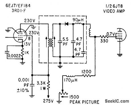
Variable resistor in video detector load circuit can be adjusted to improve snowy pictures in fringe areas.-Tv Set Size Shrinks, Electronics, 36:23, p 22.
(View)
View full Circuit Diagram | Comments | Reading(739)
AUDIO_DITHERIZING_CIRCUIT_FOR_DIGITAL_AUDIO_USE
Published:2009/7/9 1:47:00 Author:May


By adding a small amount of noise to a signal to be digitized (about 0.7 bit):
where: n=# of bits. For example, 8 bits and 2 V p-p would be 0.0055 V.
This circuit uses a transistor (Q1) and an amplifier (Q2 and U1) to generate controls the noise signal,R11 controls the noise injection and R12 controls the gain of the system. (View)
View full Circuit Diagram | Comments | Reading(825)
HEART_STIMULATING_PULSE_OUTPUT_STAGE
Published:2009/7/20 20:42:00 Author:Jessie

Used in conjunction with pulse amplifier to increase stimulating voltage when scar tissue develops under electrodes sewn to auricle and ventricle of heart, introducing excessive load resistance. Produces constant-voltage positive-going pulse having maxi-mum amplitude of 15 V and0.1-sec duration, when triggered by positive pulse.-G. F. Vanderschmidt, Two-Transistor Amplifier Corrects Heart Block, Electronics, 31:47, p 80-81. (View)
View full Circuit Diagram | Comments | Reading(845)
SCR_RELAXATION_OSCILLATOR
Published:2009/7/9 1:45:00 Author:May

View full Circuit Diagram | Comments | Reading(1258)
EEG_WAVEFORM_ANALYZER
Published:2009/7/20 20:40:00 Author:Jessie
Uses derivative curves of primary eeg signals to quantitatively describe waveshape deviations of irregular electrical waveforms emitted by brain, in terms of time and amplitude. Oporates on zero-crossing detector measurements to produce analog voltages proportional to time between base periods and also proportional to time values of left and right deviation coefficients.-C. J. Zaander, Computer Ancalyzes Brain Waveforms, Electronics, 31:29, p 68-72. (View)
View full Circuit Diagram | Comments | Reading(2772)
FLASH_METER
Published:2009/7/9 1:44:00 Author:May

Insulated-gate, field-effect transistor (IGFET), Q2 and silicon photo cell Z1 form the heart of this circuit. Transformer T1 is an audio-output type, but it's reversed in the circuit. A sudden flash from a photoflash unit detected by Z1 sends a voltage pulse through the low-impedance winding of T1 via R1. That voltage pulse is stepped-up in T1's 500-Ω, primary winding before being rectified by Q1. Transistor Q1 is used as a diode; its emitter lead was snipped off close to the case. Q1 then charges C1 to a value proportional to the amplitude of the electrical pulse generated by the light from a flash unit.
Capacitor C1 controls the current flowing through Q2, which has a very high-input impedance. The current through Q2 is read by meter Ml, a 0-50 μA dc unit, which has been calibrated in f-stops. The extremely high internal resistances of Q1 and Q2 will allow C1 to retain its charge for several minutes; this is more than enough time for you to take your reading of M1. The charge on C1 is shorted to ground and returned to 0 V by depressing reset button S1. The flashmate is ready to read the next photoflash. Trim potentiometers, R7 through R14, are adjusted to values which will yield correct readings for corresponding film sensitivities, or exposure indexes. (View)
View full Circuit Diagram | Comments | Reading(757)
DOWN_TO_005_OHM
Published:2009/7/20 20:40:00 Author:Jessie

Switch S3 gives choice of three ranges in linear ohmmeter circuit developed for measuring very small values of resistance. Values of R4, R5, and R6 require adjustment during initial calibration.-Circuits, 73 Magazine, June 1975, p 161. (View)
View full Circuit Diagram | Comments | Reading(2217)
XOR_GATE_OSCILLATOR
Published:2009/7/9 1:44:00 Author:May

An exclusive-OR gate, IC1D, turns a simple CMOS oscillator into an FSK generator. When the data input increases, IC1D inverts, and negative feedback through R2 lowers the circuit's output frequency. A low input results in positive feedback and a higher output frequency. R1 and C set the oscillator's frequency range, and R2 determines the circuit's frequency shift. To ensure frequency stability, make R3 much greater than R1 and use a high-quality feedback capacitor. The three gates constituting the oscillator itself need not be exclusive-OR types; use any CMOS inverter. (View)
View full Circuit Diagram | Comments | Reading(1311)
CMOS_OSCILLATOR
Published:2009/7/9 1:43:00 Author:May

This circuit is guaranteed to oscillate at a frequency of about 2.2/(R1 ×C) if R2 is greater than R1 You can reduce the number of gates further if you replace gates 1 and 2 with a noninverting gate. (View)
View full Circuit Diagram | Comments | Reading(0)
TWO_SALLEN_KEY_LOW_PASS_ACTIVE_FILTERS
Published:2009/7/9 1:43:00 Author:May

These filters are designed for 10-kΩ impedance level and 1-kHz cutoff frequency, but the components can be scaled as required for other impedances and cutoff frequencies. (View)
View full Circuit Diagram | Comments | Reading(813)
WIEN_BRIDGE_OSCILLATOR
Published:2009/7/9 1:42:00 Author:May

LEDs function as both pilot lamps and as an AGC (automatic gain control) in this unconventional amplitude-stabilized oscillator. (View)
View full Circuit Diagram | Comments | Reading(0)
VIDEO_GAIN_BLOCK
Published:2009/7/9 1:41:00 Author:May


This configuration utilizes the wide bandwidth and speed of HA-2540, plus the output capability of HA-5033. Stabilization circuitry is avoided by operating HA-2540 at a closed loop gain of 10, while maintaining an overall block gain of unity. However, gain of the block can be varied using the equation:A maxlmum block gam of 3is recommended to prevent signal distortinThis ciruit was tested for differential phase and differential gatn using a Tektronix 520A vector scopeand a Tektronix 146 video signal generator Both differential phase and differential gain were too small tobe measured. (View)
View full Circuit Diagram | Comments | Reading(582)
DARKROOM_ENLARGER_TIMER
Published:2009/7/9 1:41:00 Author:May

The NE555 circuit is a basic one-shot timer with a relay connected between the output and ground. It is triggered with the normally open momentary contact switch, which when operated, grounds the trigger input at pin 2. This causes a high output to energize K1 which closes the normally open contacts in the lamp circuit. They remain closed during the timing interval, then open at time out. Timing is controlled by a 5-MΩ potentiometer, Rt. All timerdriven relay circuits should use a reverse clamping diode, such as D1, across the coil. The purpose of diode D2 is to prevent a timer output latch-up condition in the presence of reverse spikes across the relay.With the rc time constant shown, the full-scale time is about 1 minute. A scale for the 5-MΩ potenti-ometer shaft position can be made and calibrated in seconds. Longer or shorter full-scale times can be achieved by changing the values of the rc timing components. (View)
View full Circuit Diagram | Comments | Reading(1309)
_QUADRATURE_OSCILLATOR
Published:2009/7/9 1:41:00 Author:May

View full Circuit Diagram | Comments | Reading(606)
LOW_FREQUENCY_OSCILLATOR
Published:2009/7/9 1:40:00 Author:May


This simple rc oscillator uses a medium-speed comparator with hysteresis and feedback through R1 and C1 as timing elements. The frequency of oscillation is, at least theoretically, independent from the power supply voltage. If the comparator swings to the supply rails, if the pull-up resistor is much smaller than the resistor Rh, and if the propagation delay is negligible compared to the rc time constant, the oscillation frequency is: (View)
View full Circuit Diagram | Comments | Reading(105)
| Pages:914/2234 At 20901902903904905906907908909910911912913914915916917918919920Under 20 |
Circuit Categories
power supply circuit
Amplifier Circuit
Basic Circuit
LED and Light Circuit
Sensor Circuit
Signal Processing
Electrical Equipment Circuit
Control Circuit
Remote Control Circuit
A/D-D/A Converter Circuit
Audio Circuit
Measuring and Test Circuit
Communication Circuit
Computer-Related Circuit
555 Circuit
Automotive Circuit
Repairing Circuit