
Circuit Diagram
Index 901
SUPPLY_VOLTAGE_SPLITTER
Published:2009/7/9 4:02:00 Author:May

This simple circuit can convert a single supply voltage, such as a battery, into a bipolar supply. Sense resistors R1 and R2 establish relative magnitudes for the resulting positive and negative voltages. Their rail-to-rail value, of course, equals VSUPPLY. R4 and R5 represent the load impedances. For example, equalvalue sense resistors produce 1/2 VSUPPLY across each of the load resistors, R4 and R5. The op amp maintains these equal voltages by sinking or sourcing current through R3; the op amp's action is equivalent to that of variable conductances G1 and G2 in shunt with each load resistor. Choose a value for R3 so that the largest voltage across it, the greatest load-current mismatch, won't exceed the op amp's output-voltage capability for the application. You can add a buffer amplifier at the op amp's output to provide greater load currents. If you need bypass capacitors across the load resistors as well, connect a capacitor (dashed lines) to ensure that the amplifier remains stable. (View)
View full Circuit Diagram | Comments | Reading(714)
150_AND_300_V_SERIES_TUBE_REGULATOR
Published:2009/7/20 6:45:00 Author:Jessie
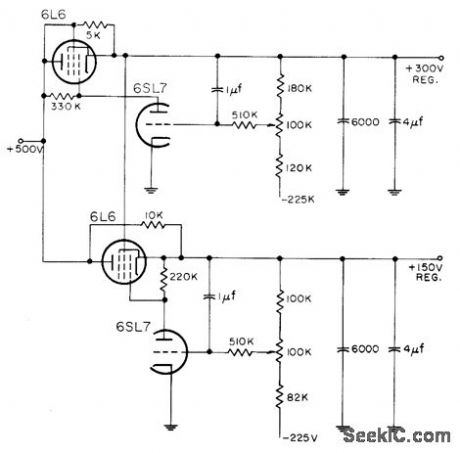
Uses simple triode as regulator amplifier. Series tube for 300.v supply is conventional triode-connected pentode, but series tube that regulates 150 v has its screen fed from output of 300-v regulated supply, for pentode operation.-NBS, Handbook Preferred Circuits Navy Aeronautical Electronic Equipment, Vol. 1, Electron Tube Circuits, 1963, p N2-11. (View)
View full Circuit Diagram | Comments | Reading(1646)
AC_VOLTAGE_REGULATOR
Published:2009/7/9 4:01:00 Author:May

View full Circuit Diagram | Comments | Reading(705)
BF_IF_amplifier_for_30_MHz_60_MHz_100_MHz
Published:2009/7/20 6:44:00 Author:Jessie

BF-IF amplifier for 30 MHz/60 MHz/100 MHz (courtesy Motorola Semiconductor Products Inc.). (View)
View full Circuit Diagram | Comments | Reading(1101)
SLOW_TURN_ON_15_V_REGULATOR
Published:2009/7/9 4:00:00 Author:May

View full Circuit Diagram | Comments | Reading(895)
POTENTIOMETER_POSITION_V_F_CONVERTER
Published:2009/7/9 3:59:00 Author:May

In this application, an AD652IC is used in a synchronized V/F converter that derives its input from the position of a potentiometer. This can represent a position of a mechanical component, weight, size, etc., to give a 0-to-100-kHz output versus the 0-to-5-V output from the potentiometer.
(View)
View full Circuit Diagram | Comments | Reading(1049)
THERMOCOUPLE_VACUUM_GAGE_HEATER
Published:2009/7/20 6:43:00 Author:Jessie

Simple regulator for 240-v d-c supply provides 140 mc with 0.1% regulation. Uses regulator triode, pentode-connected d-c amplifier, and series-connected reference regulator tube.-W. V. Loebenstein, Regulated Power Supply for Instruments, Electronics, 33:48, p 132. (View)
View full Circuit Diagram | Comments | Reading(2137)
SHUNT_REGULATOR
Published:2009/7/20 6:41:00 Author:Jessie
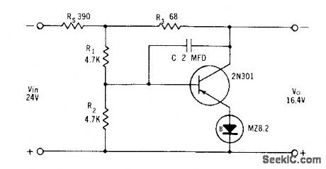
Used when output volt-age must be higher than zener voltage. Rip-ple is less than 10 my when regulator is supplied by full-wove rectifier having 20 mid capacitance.- Zener Diode Handbook, In ternational Rectifier Corp., 1960, p 55. (View)
View full Circuit Diagram | Comments | Reading(811)
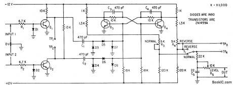
HIGH_CURRENT_INDUCTOULESSSWITCHING_REGULATOR
Published:2009/7/9 3:59:00 Author:May


The LTC10432 switched-capacitor building block provides nonoverlapping complementary drive to the Q1 to Q4 power MOSFETs. The MOSFETs are arranged so that C1 and C2 are altemately placed in series and then parallel. During the series phase, the + 12 V battery's current flows through both capacitors, charging them, and fumishing load current. During the parallel phase, both capacitors deliver current to the load. Q1 and Q2 receive similar drive from pins 3 and 11. The diode-resistor networks provide additional nonoverlapping drive characteristics, preventing simultaneous drive to the series-parallel phase switches. Normally, the output would be one-half of the supply voltage, but C1 and its associated compo-nents close a feedback loop, forcing the output to 5 V. With the circuit in the series phase, the output heads rapidly positive. When the output exceeds 5 V, C1 trips, forcing the LTC1043 oscillator pin, trace D, high; this truncates the LTC1043's triangular-wave oscillator cycle. The circuit is forced into the parallel phase and the output coasts down slowly, until the next LTC1043 clock cycle begins. C1's output diode prevents the triangle down-slope from being affected and the 100-pF capacitor provides sharp transitions. The loop regulates the output to 5 V by feedback controlling the turn-off point of the series phase. (View)
View full Circuit Diagram | Comments | Reading(596)
PHASE_DIFFERENCE_METER_FOR_02_TO_20_KC_
Published:2009/7/20 6:34:00 Author:Jessie
Measures phase difference between two sinusoidal inputs. Each limiter (Q1 and Q2) drives one side of high-speed flip-flop Q3-Q4 through differentiating and clipping circuits, giving square wave that turns on when one input signal goes negative and turns off when other input goes negative. D-c value of output voltage is proportional to phase difference, with about 11 V corresponding to 360°.-J. R. Woodbury, Measuring Phase with Transistor Flip-Flops, Electronics, 34:38, p 56. (View)
View full Circuit Diagram | Comments | Reading(615)
LOGARITHMIC_SWEEP_VCO
Published:2009/7/9 3:58:00 Author:May

This circuit uses the output of the ICL8049 to control the frequency of the ICL3038 waveform genera-tor; the 741 op amp is used to linearize the voltage-frequency response. The input voltage to the 8049 can be, for example, from the horizontal sweep signal of an oscilloscope; the output of the 8038 will then sweep logarithmically across the audio range. By feeding this to the equipment being measured and detecting the output, a standard frequency response can be obtained. If the output is fed through an ICL8048 before being displayed, a standard bode plot results. (View)
View full Circuit Diagram | Comments | Reading(1970)
SMALLEST_PHASE_CONTROL
Published:2009/7/20 6:32:00 Author:Jessie

Miniature lamp No. 2128 with small, low-mass filament can reach firing level of light-activated scr in about three cycles with low applied voltage. As applied voltage is increased, this time is reduced to about 1 millisec when lamp is directed across LASCR terminals, thus providing phase control. Lamp voltage is removed when LASCR fires, protecting lamp and resetting it for next half-cycle. Useful for dimming 25-w lamp or for controlling temperature of small soldering iron.- Silicon Controlled Rectifier Manual, Third Edition, General Electric Co., 1964, p 213. (View)
View full Circuit Diagram | Comments | Reading(719)
POSITIVE_REGULATOR_WITH_NPN_AND_PNP_BOOST
Published:2009/7/9 3:56:00 Author:May

In the circuit, Q1 and Q2 are connected in the classic SCR or thyristor configuration. Where higher input voltages or minimum component count are required, the circuit for thyristor boost can be used. The thyristor is running in a linear mode with its cathode as the control terminal and its gate as the output terminal. This is known as the remote base configuration. (View)
View full Circuit Diagram | Comments | Reading(625)
10_MHz_RF_amplifier_using_an_ECG703A_IC
Published:2009/7/20 6:29:00 Author:Jessie
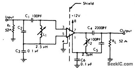
10 MHz RF amplifier using an ECG703A IC. The input signal is coupled to the amplifier through tank L1-C1-C2, tuned to 10 MHz. The capacitive divided C1-C2 provides impedance matching. Network L2-C4-C5 connects the amplifier to the load. A shield should be used between the input and output to prevent oscillations (courtesy GTE Sylvania Incorporated). (View)
View full Circuit Diagram | Comments | Reading(909)
FUNCTION_GENERATOR
Published:2009/7/9 3:56:00 Author:May

Using an Intersil ICL8038, this function generator generates frequencies from 1 Hz to over 80 kHz.R1 is the fine frequency control and S1 is the coarse frequency control range switch. S2 selects square-, triangle-, or sine-wave output. U2 is a buffer amplifier and R5 sets output level. R2 is adjusted for a sym-metrical triangle wave. R3 and R4 are adjusted for minimum sine-wave distortion. Power supply is ±12 V at less than 100 mA. (View)
View full Circuit Diagram | Comments | Reading(0)
250_MHz_PF_to_50_MHz_IF_mixer_using_an_MM1941_transistor
Published:2009/7/20 6:28:00 Author:Jessie

250 MHz PF to 50 MHz IF mixer using an MM1941 transistor. The external local oscillator injection frequency is 300 MHz. The output of the mixer is tuned to the difference between the two inputs (courtesy Motorola Semiconductor Products Inc.). (View)
View full Circuit Diagram | Comments | Reading(799)
5_V_TO_ISOLATED_5_V_AT_20_MA_CONVERTER
Published:2009/7/9 3:55:00 Author:May

In this circuit, a negative output voltage dc-dc converter generates a -5 V output at pin A. In order to generate - 5 V at point A, the primary of the transformer must fly back to a diode drop more negative than -5 V. If the transformer has a tightly coupled 1/1 turns ratio, there will be a 5 V plus a diode drop across the secondary. The 1N5817 rectifies this secondary voltage to generate an isolated 5-V output. The isolated output is not fully regulated since only the -5 V at point A is sensed by the MAX635. (View)
View full Circuit Diagram | Comments | Reading(1605)
EFFICIENT_NEGATIVE_VOLTAGE_REGULATOR
Published:2009/7/9 3:54:00 Author:May

One way to provide good negative-voltage regulation is with a low-dropout positive-voltage regulator operating from a well-isolated secondary winding of switch-mode circuit transformer. The technique works with any positive-voltage regulator, although highest efficiency occurs with low-dropout types.Under all loading conditions, the minimum voltage difference between the regulator VIN and V0UT pins must be at least 1.5V, the LT1086's low-dropout voltage. If this requirement isn't met, the output falls out of regulation. Two programming resistors, R1 and R2, set the output voltage to 12 V, and the LT1086's servo the voltage between the output and its adjusting (ADJ) terminals to 1.25 V. Capacitor C1 improves ripple rejection, and protection diode D1 eliminates common-load problems.Since a secondary winding is galvanically isolated, a regulator's 12 V output can be referenced to ground. Therefore, in the case of a negative-voltage output, the positive-voltage terminal of the regulator connects to ground, and the -12 V output comes off the anode of D1. The VIN terminal floats at 1.5 V or more above ground. (View)
View full Circuit Diagram | Comments | Reading(2168)
30_MHz_PF_amplifier_using_an_ECG703A_IC
Published:2009/7/20 6:27:00 Author:Jessie
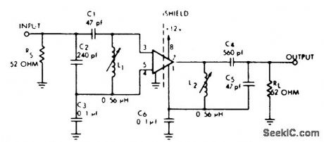
30 MHz PF amplifier using an ECG703A IC. The input signal is coupled through tank L1-C1-C2 to the ECG703A. Capacitors C1 and C2 form an impedance matching network. Network L2- C4- C5 coupled the output signal to the load. Use a shield between the input and output to prevent spurious oscillations (courtesy GTE Sylvania Incorporated). (View)
View full Circuit Diagram | Comments | Reading(848)
NONLINEAR_PORENTIOMER_OUTPUTS
Published:2009/7/9 3:53:00 Author:May

Using these illustrated conftgurations, various rotation output characteristics can be obtained from potentiometers and one or two resistors. (View)
View full Circuit Diagram | Comments | Reading(506)
| Pages:901/2234 At 20901902903904905906907908909910911912913914915916917918919920Under 20 |
Circuit Categories
power supply circuit
Amplifier Circuit
Basic Circuit
LED and Light Circuit
Sensor Circuit
Signal Processing
Electrical Equipment Circuit
Control Circuit
Remote Control Circuit
A/D-D/A Converter Circuit
Audio Circuit
Measuring and Test Circuit
Communication Circuit
Computer-Related Circuit
555 Circuit
Automotive Circuit
Repairing Circuit