
Circuit Diagram
Index 908
O_TO_200_nA_CURRENT_SOURCE
Published:2009/7/9 2:32:00 Author:May

This circuit uses readily available parts to implement a 0-to-200-nA current source. The circuit bor-rows a PMOS transistor from the input stage of a DC4007A, which is easier to obtain than a discrete PMOS transistor. The CA3130 op amp operates as a follower so that its positive input sets the current that flows through R2. The MOSFET input stage of this op amp exhibits low-input current. The op amp must be able to produce an output voltage high enough to turn the CD4007A's internal FET off. Thus, the op amp requires a positive supply voltage of 5 V. The circuit presents an output voltage from 0 to 3 V, and R1 controls the amount of output current.
(View)
View full Circuit Diagram | Comments | Reading(1551)
TRIGGER_SHAPING_FOR_RETINA_WELDER
Published:2009/7/20 20:23:00 Author:Jessie
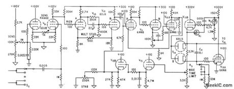
Trigger pulse, selected by S2, is compared to fixed bias on one half of comparator tube V9. Trigger shaping by V10 provides strong, sharp pulse for gating mvbr V11-V12A, which turns off diodes V14, allowing Miller integrator V13A and cathode follower V13B to start lime base runup that drivesC4 to 150V. Circuit then reverts to normal.-O. Rich, Jr. and R. V. Hill, R-F Spot Welder Reattaches Retina of Human Eye, Electronics,34:32, p 160-163. (View)
View full Circuit Diagram | Comments | Reading(678)
VIDEO_PALETTE
Published:2009/7/9 2:31:00 Author:May
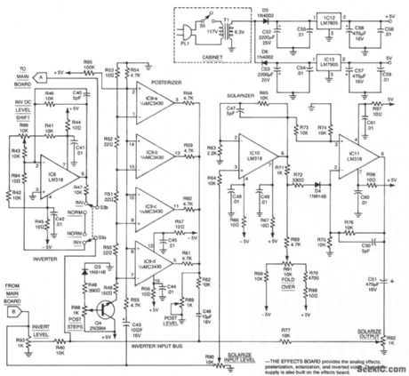
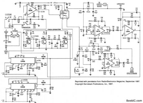
This system consists of two parts. The main board dissects the video signal and provides independent level control for burst, chroma, luminance, and sync signals, as well as phase and polarity. The video signal is reassembled in the output in corrected or modified format as required by the user. The effects board produces luminance inversion or can generate discrete luminance steps (posterization) or a nonlinear gray scale (solarization) to achieve simulation of photographic effects commonly seen in various special-effect photographic processes. The kit is available from North Country Radio, P.0. Box 53, Wykagyl Station, NY 10804. (View)
View full Circuit Diagram | Comments | Reading(1859)
105_MHz_low_noise_BF_amplifier_using_a_3N204_dual_gate_MOSFET
Published:2009/7/20 20:22:00 Author:Jessie

105 MHz low-noise BF amplifier using a 3N204 dual-gate MOSFET (courtesy Texas tnstruments tncorporated). (View)
View full Circuit Diagram | Comments | Reading(956)
3_V_WATER_LEVEL_DETECTOR
Published:2009/7/9 2:31:00 Author:May

Originally, this circuit was used to sense a low-water level in a Christmas tree stand, but the circuit can be used as a water-level detector for pump controls, water sensors (for garden and lawn applications), etc.A comparator and probe setup with a Linear Technology LTC1040CN comparator drives a 2N3906, which switches a tone generator. Sampling occurs every 20 seconds, which minimizes current drain. A pair of dry cells will power the circuit for several months. (View)
View full Circuit Diagram | Comments | Reading(1104)
900_MHz_to_45_MHz_converter_using_dual_gate_3N204_MOSFETs_and_a_2N5245
Published:2009/7/20 20:21:00 Author:Jessie

900 MHz to 45 MHz converter using dual-gate 3N204 MOSFETs and a 2N5245 (courtesy Texas Instruments mcorporated). (View)
View full Circuit Diagram | Comments | Reading(993)
GENERAL_PURPOSE_5_W_AUDIO_AMPLIFIER_WITH_ac_POWER_SUPPLY
Published:2009/7/9 2:31:00 Author:May

This general-purpose low-power (5 W) audio amplifier is suitable for driving a speaker of approxi-mately 8 to 12 inches. A Sanyo LA4460 IC is used as the audio output IC. The circuit consists of a loud-ness control, driver amplifier Q1, and bass and treble controls of about ±10 dB boost/cut. It should be useful in a wide variety of situations. Either the ac supply shown can be used, or a 12 Vdc supply can be connected to points A&B (positive) and C (negative). Two of these circuits, using ganged potentiometers at R2, R7, and R11 can be used for stereo applications. T1 is a 12-V 1-amp plug-in transformer. Notice that IC1 must be heatsinked. Power output is about 5 W. A 4 x2 x0.050 aluminum heatsink should be adequate. (View)
View full Circuit Diagram | Comments | Reading(1406)
27_MHz_to_45_MHz_converter_using_two_3N204_MOSFETs_
Published:2009/7/20 20:20:00 Author:Jessie

27 MHz to 45 MHz converter using two 3N204 MOSFETs (courtesy Texas Instruments Incorporated). (View)
View full Circuit Diagram | Comments | Reading(1558)
VARIABLE_VOLTAGE_REFERENCE_SOURCE
Published:2009/7/9 2:30:00 Author:May
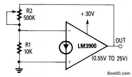


The noninverting terminal of the op amp is grounded, and the circuit uses the voltage at the inverting terminal as a reference. Its voltage gain is determined by the R2/R1ratio. When R2 is set at zero, the circuit has unity gain and a 0.55-V output. When R2 is set to the maximum value, the circuit has a gain of 50 and an output of about 25 V. The circuit provides good regulation and can supply output currents of several milliamps. The output voltage however, is not temperature compensated. (View)
View full Circuit Diagram | Comments | Reading(749)
LOW_COST_LOW_DROPOUT_LINEAR_REGULATOR
Published:2009/7/9 2:29:00 Author:May
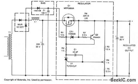
This linear post regulator provides 12 V at 3 A. It employs TL431 reference U1 which, without additional amplification, drives TMOS MTP3055A gate Q1 series pass regulator. Bias voltage is applied through R1 to Q1's gate, which is protected against overvoltage by diode CR1. Frequency compensation for closed-loop stability is provided by C1.Key performance features are: Dropout voltage: 0.6 V Load regulation: 10 mV Line regulation:±5 mV Output ripple: 10 mV pk-pk (View)
View full Circuit Diagram | Comments | Reading(2250)
WATER_LEVEL_CONTROL
Published:2009/7/9 2:28:00 Author:May
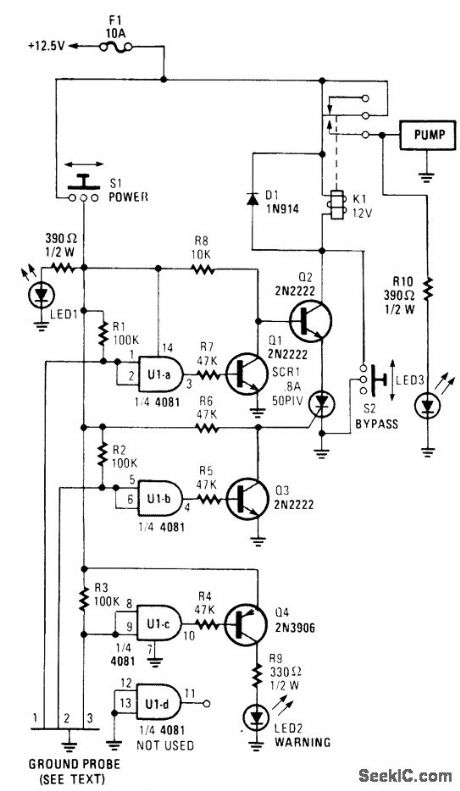
This circuit will power up a water pump when the water reaches a predetermined level. Then it turns itself off when the water recedes to another predetermined point.
Gates U1A through U1C each have their two inputs tied together, and serve as probes. The probes are then placed at various levels to trigger a particular function at a predetermined time. The ground side of the circuit is placed below the mini-mum water level. The inputs to each gate are tied high through a 100-kΩ resistor connected to the +12.5-V bus.
As the water level slowly rises to probe L, the input to U1A is pulled low by the conduction of current through the water to the ground probe. That turns Q1 off and Q2 on. With Q2 turned on, the ctr-cuit is placed in the standby mode, ready to activate the pump when conditions are right.
Probe 2 is placed at the maximum water level.If the water level reaches probe 2, the input of U1B is brought low, turning Q3 on, which, in tum, causes current to be applied to the gate of SCR1, turning it on. The circuit through K1, Q2, and SCR1 is now complete to ground, and the water pump is now turned on, which causes the water level to recede. When the water level falls below probe 2, U1B goes back to logic high.
However, because of the latching nature of SCR1, the pump continues to run until the water level falls below probe 1. At that point, the ground circuit opens and de-energizes K1, which turns the pump off. The pump will not tum on again until the water level again rises above probe 2.
Probe 3 was added as a warning. If the water level reaches probe 3, LED2 indicates that the pump is not working. Switch S2 is a manual over-ride and S1 powers the sensing circuit. LED3 indi-cates that power has been applied to the pump.LED1 indicates that power has been applied to the sensor. (View)
View full Circuit Diagram | Comments | Reading(0)
FET_VOM
Published:2009/7/20 20:17:00 Author:Jessie

Use two FETs in balanced circuit. Meter reads zero when circuit is balanced with R11. Values being measured produce imbalance linearly proportional to output voltage of bridge. Resistance measurements use linear ohms-readout system, with single meter scale serving for all resistance and voltage measurements. In ohms position, meter will rest gently against peg at high end of scale. When ohmmeter leads are shorted, zero pot is adjusted so meter reads 0 ohms. Article covers construction and calibration.-J. Rusgrove, An FET Volt-Ohmmeter with Linear Ohms Readout, QST, March 1978, p 16-18. (View)
View full Circuit Diagram | Comments | Reading(3153)
SWITCHING_POWER_SUPPLY
Published:2009/7/9 2:26:00 Author:May
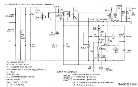
This low-voltage high-current output, switching dc power supply is running off the 220-Vac input. In this circuit, an ST2 diac relaxation oscillator, Q3, C1, and the diac, initiates conduction of the output switching transistor Q1, the on-time of which is maintained constant by a separate timing/commutation network consisting of Q2, C2, SUS, and SCR 1. The output voltage, consequently, is dependent on the duty cycle. To compensate for unwanted variations of output voltage because of input voltage or load resistance fluctuations, an H11C wired as a linear-model unilateral PNP transistor in a stable differential amplifier configuration is connected into the galvanically isolated negative-feedback loop. The loop determines the duty cycle and hence the output voltage. Of further interest in this circuit is the use of several low-current, high-voltage, 400VDRM thyristors (Q2, Q3,) which are also used as pnp remote-base transistors. Short-circuit protection is assured by coupling Q1 collector-current feedback into the turn-off circuitry via RSS. (View)
View full Circuit Diagram | Comments | Reading(0)
THREE_RANGE_MILLIOHMM_ETER
Published:2009/7/20 20:16:00 Author:Jessie

Solid-state design measures resistance values accurately down to less than 0.001 ohm. Full-scale values for ranges are 10, 1, and 0.1 ohms.-Circuits, 73 Magazine, July 1974, p 80. (View)
View full Circuit Diagram | Comments | Reading(1343)
12_V_2O_W_STEREO_AMPLIFIER
Published:2009/7/9 2:26:00 Author:May
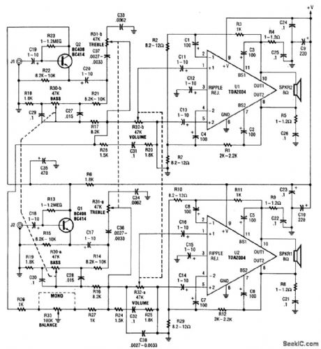
This amplirier 20W per channel. Input sensitivity is about 300mV into 47kΩ. Notice that a bridged output is used,so the speakers are operated with both wires above ground.A + 12-V supply is used. U1 and U2 must be heatsinked. (View)
View full Circuit Diagram | Comments | Reading(736)
LINEAR_SCALE_OHMMETER
Published:2009/7/20 20:14:00 Author:Jessie

Unknown resistance value is arithmetic product of standard resistor value and current reading in milliam-peres. With 1K standard resistor, deflections from 0 to 1 A correspond to resistance readings from 0 to 1K. Requires no calibration and no zero adjustment. Can be made multirange by switching in different standard resistors.-J.Schultz, An Ohmmeter Potpourri, CQ, June 1978, p 32-33. (View)
View full Circuit Diagram | Comments | Reading(0)
PROGRAMMABLE_IDENTIFIER
Published:2009/7/9 2:24:00 Author:May

Used on an amateur or experimental radio beacon,the above ID circuit will generate any callsign or message programmed into the EPROM. A CD4020 CMOS counter is driven by an RC clock circuit.This addresses the EPROM.and serial data is available at pin 9. (View)
View full Circuit Diagram | Comments | Reading(1996)
WATER_SEEPAGE_ALARM
Published:2009/7/20 20:12:00 Author:Jessie

National LM3909 flasher IC operating from 1.5-V cell provides safe water-seepage alarm for potentially damp floors because there is no connection to power line, When sensing electrodes pass about 0.25μA through moisture, pair of 2N2484 transistors (QA and QB) become astable MVBR operating at rate that starts at 1 Hz and increases with leakage between electrodes. Pulse waveform applied to pin 8 of IC varies timing current of flasher, resulting in distinctively modulated tone output for loudspeaker of alarm. Sensors can be two strips of stainless steel on insulators or zigzag path in copper of printed-wiring board. Place damp finger across gap to test alarm.-P. Lefferts, Power-Miser Flasher IC Has Many Novel Applications, EDN Magazine, March 20, 1976, p 59-66. (View)
View full Circuit Diagram | Comments | Reading(0)
VIDEO_SWITCH_WITH_VERY_HIGH_OFF_ISOLATION
Published:2009/7/9 2:22:00 Author:May
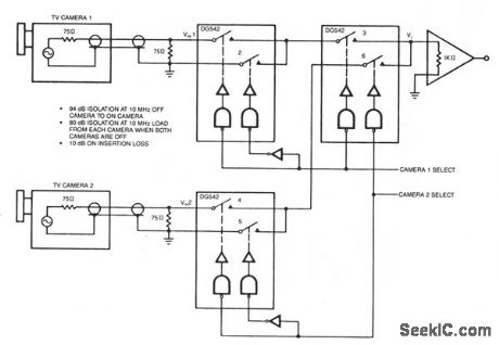
View full Circuit Diagram | Comments | Reading(590)
WIRELESS_VIDEO_CAMERA_LINK
Published:2009/7/9 2:21:00 Author:May
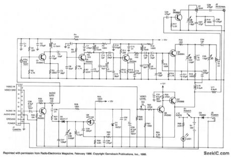
This high-performance video-camera link transmits signals from your video camera to your VCR, or from your VCR to TVs throughout your home. The first stage of the rf chain is a crystal-controlled oscillator, Q1, with a frequency of 60 to 65 MHz, which is one-eighth of the final output frequency. The oscillator produces a signal of about +6 dBm (4 mW) that drives three stages of frequency doublers. The combined action of those doublers multiplies the input frequency by eight for a final output frequency of (nominally) 500 MHz. Double-tuned circuits are used between each stage to help reduce spurious outputs that might cause unwanted interference. The video input signal from your VCR, video camera, etc. drives a video modulator, Q6 and Q7, that adds the video signal to the + 12 V line supplying power to the final doubler, Q4, and the output amplifier, Q5. That method of modulation is similar to the way a conventional AM-radio transmitter is modulated. The video modulator has a nominal bandwidth of five MHz. The audio input is applied to Q8, which operates as a VCO running at a nominal frequency of 4.5 MHz to produce the modulated sound carrier. For simplicity, Q8 is a free-running oscillator, since the ±25 kHz frequency deviation that is required would be very difficult to produce at that frequency with a crystal-controlled oscillator. Besides, most TV sound systems will accept a ± 10 kHz error in the sound-carrier frequency without producing undue distortion, and that greatly simplifies the circuitry required. The kit is available from North Country Radio, P.O. Box 53, Wykagyl Station, NY 10804. (View)
View full Circuit Diagram | Comments | Reading(862)
| Pages:908/2234 At 20901902903904905906907908909910911912913914915916917918919920Under 20 |
Circuit Categories
power supply circuit
Amplifier Circuit
Basic Circuit
LED and Light Circuit
Sensor Circuit
Signal Processing
Electrical Equipment Circuit
Control Circuit
Remote Control Circuit
A/D-D/A Converter Circuit
Audio Circuit
Measuring and Test Circuit
Communication Circuit
Computer-Related Circuit
555 Circuit
Automotive Circuit
Repairing Circuit