
Circuit Diagram
Index 904
VOLTAGE_CONTROLLED_CURRENT_SOURCE_WITH_GROUNDED_SOURCE_AND_LOAD
Published:2009/7/9 3:13:00 Author:May
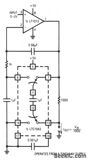
This is a simple, precise voltage-controlled current source. Bipolar supplies will permit bipolar output. Conftgurations featuring a grounded voltage-control source and a grounded load are usually more complex and depend upon several components for stability. In this circuit, accuracy and stability almost entirely depend upon the 100-Ω shunt. (View)
View full Circuit Diagram | Comments | Reading(607)
ELECTRIC_GUITAR_MATCHING_AMPLIFIER
Published:2009/7/9 3:13:00 Author:May
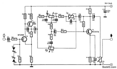
An electric guitar often has to be connected to a mixing panel, a tape deck or a potable studio. As far as cabling is concerned, that is no problem, but matching the high impedance of the guitar element to the low impedance of the line input of the mixing panel or tape deck is a problem. Even the so-called high impedance inputs of those units are not suitable for the guitar output. When the guitar is connected to such an input, hardly any signal is left for the panel or deck to process.
It would be possible to connect the guitar to the (high impedance) microphone input, but it is normally far too sensitive for that purpose; guitar clipping occurs all too readily.
The matching amplifier presented here solves those problems: it has a high-impedance (1 MΩ) input that can withstand voltages of over 200 V. The output impedance is reasonably low. Amplification is x 2 (6 dB). Dual tone control, presence control, and volume control are provided.
The circuit can handle input levels of up to 3 V. Above that level distortion increases, but that is, of course, a good thing with guitar music. Real clipping of the input signal does not occur until much higher levels than are obtainable from a guitar are applied. Power is supplied by a 9-V (PP3) battery from which the circuit draws a current that does not exceed 3 mA. (View)
View full Circuit Diagram | Comments | Reading(1226)
HIGH_STABILITY_10_V_REGULATOR
Published:2009/7/9 3:12:00 Author:May

View full Circuit Diagram | Comments | Reading(569)
WATER_LEAK_ALARM
Published:2009/7/9 3:12:00 Author:May
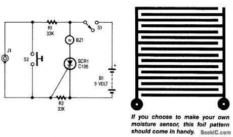
A sensor connected to J1 causes SCR1 to conduct, which sounds buzzer BZ1. The sensor is a PC-board foil pattern grid. Several sensors can be wired in parallel for increased coverage or to monitor sev-eral places simultaneously. (View)
View full Circuit Diagram | Comments | Reading(823)
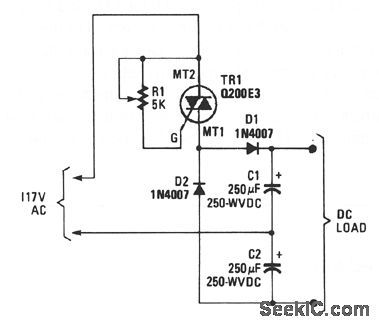
TRIAC_CONTROLLED_VOLTAGE_DOUBLER
Published:2009/7/9 3:11:00 Author:May
View full Circuit Diagram | Comments | Reading(713)
PROGRAMMABLE_POWER_SUPPLY
Published:2009/7/9 3:10:00 Author:May
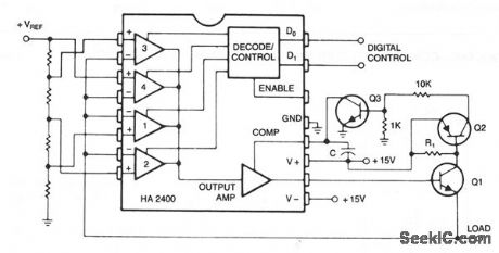
Many systems require one or more relatively low-current voltage sources which can be programmed to a few predetermined levels. The circuit shown above produces positive output levels, but could be modified for negative or bipolar outputs. Q1 is the series regulator transistor, selected for the required current and power capability. R1, Q2, and Q3 form an optional short circuit protection circuit, with R1 chosen to drop about 0.7 V at the maximum output current. The compensation capacitor, C, should be chosen to keep the overshoot, when switching, to an acceptable level. (View)
View full Circuit Diagram | Comments | Reading(0)
HIGH_PERFORMANCE_VIDEO_SWITCH
Published:2009/7/9 3:09:00 Author:May
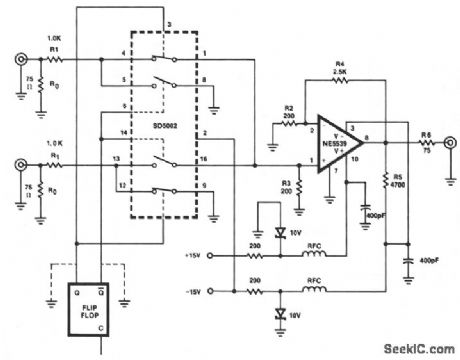
This figure shows a one-of-two switch with a summing amplifier. The video source's line can be termi-nated either externally or internally to switch R0. With this termination resistor, a load change of less than 1 Ω will be seen by the source when the switch changes state. For this reason, input isolation amplifiers are not necessary. R4 can be varied to control circuit gain, but should never be less than 1400 Ω since the NE5539 is internally compensated for gain values greater than seven. A value of approximately 2500 Ω for R4 will set circuit gain to near unity. Additionally, the circuit output impedance is set by R6, and R5 sets the output dc offset to near zero. (View)
View full Circuit Diagram | Comments | Reading(708)
LATCHING_WATER_SENSOR
Published:2009/7/9 3:09:00 Author:May

A balanced Wheatstone bridge controls a JK flip-flop that uses an op amp as an interface. This in turn drives a relay circuit. R1 through R4 can be made larger for increased sensitivity. (View)
View full Circuit Diagram | Comments | Reading(1702)
SIMPLE_MICROPHONE_PREAMP
Published:2009/7/9 3:09:00 Author:May
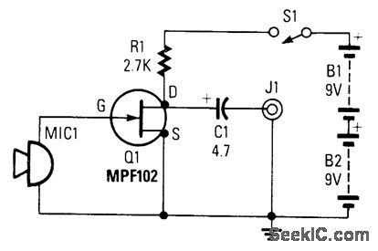
This preamp uses a small dynamic microphone coupled to the gate of Q1. R1 is a load resistor.Audio is taken out between the negative side of C1 and ground. Output will be between 10 and100 mVpp, depending on the microphone. (View)
View full Circuit Diagram | Comments | Reading(1075)
THREE_RAIL_POWER_SUPPLY
Published:2009/7/9 3:08:00 Author:May
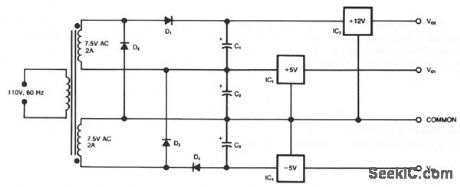
This circuit generates three supply voltages using a minimum of components. Diodes D2 and D3 perform full-wave rectification, alternately charging capacitor C2 on both halves of the ac cycle. On the other hand, diode D1 with capacitor C1, and diode D4 with capacitor C3 each perform half-wave rectification. The full- and half-wave rectification arrangement is satisfactory for modest supply currents drawn from - 5 and +12-V regulators IC3 and IC2. You can use this circuit as an auxiliary supply in an up-based instru-ment, for example, and avoid the less attractive alternatives of buying a custom-wound transformer, build-ing a more complex supply, or using a secondary winding, say 18 Vac, and wasting power in the 5-V regulators. (View)
View full Circuit Diagram | Comments | Reading(589)
LOW_NOISE_1_000×PREAMP
Published:2009/7/9 3:08:00 Author:May
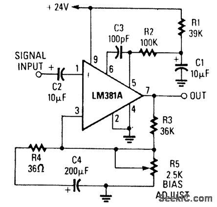
An LM381A is used here as a low-noise pre-amp with a gain of approximately 1 000 x. Adjust R5 for 12 V at pin 7, assuming a 24-V supply. (View)
View full Circuit Diagram | Comments | Reading(1361)
LOW_NOISE_AMPLIFIER
Published:2009/7/9 3:07:00 Author:May
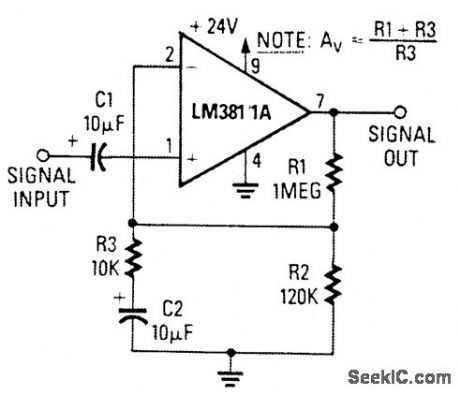
This low-noise LM381/1A noninverting ampli-fter has a gain of 100. (View)
View full Circuit Diagram | Comments | Reading(1841)
LOW_POWER_INVERTER
Published:2009/7/9 3:07:00 Author:May
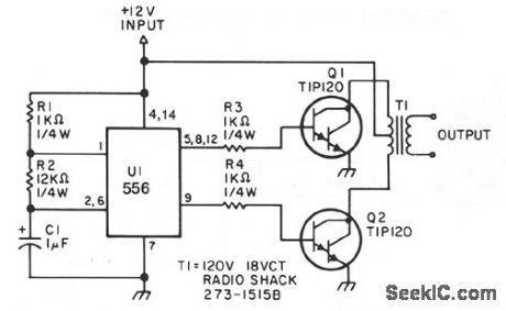
This low-power inverter uses only 9 parts and turns 10 to 16 Vdc into 60-Hz, 115-V square-wave powqr to operate ac equipment up to 25 W. The first section of the 556 timer chip is wired as an astable oscillator with R2 and C1 setting the frequency. The output is available at pin 5. The second section is wired as a phase inverter. That output is available at pin 9. Resistors R3 and R4 keep output trans;stors Q1 and Q2 from loading down the oscillator. The two transistors drive the transformer push-pull fashion.When one transistor is biased-on, the other is cut-off. The transformer is a 120 V/18 VCT unit that is connected backwards, so that it steps the voltage up rather than down. Oscillator circuit U1, R1, R2, and C1 operates from about 4 to 16 V with a very stable output. (View)
View full Circuit Diagram | Comments | Reading(743)
_4_CHANNEL_MIXERV
Published:2009/7/9 3:07:00 Author:May


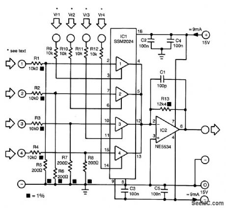

The proposed mixer is designed around four current-driven transconductance amplifiers contained in an SSM2024 from Precision Monolithics. To obtain a low offset and high control rejection, the four inputs should have an impedance to earth of about 200 Ω . These impedances are obtained from resistors R5 through R8, which also form part of a potential divider at each input.With the values in the diagram, the nominal input signal is 1 V (0 dBV). Distortion at that level is about 1%; at lower levels, it is not more than 0.3%.
The amplification of the current-driven amplifiers (CDAs) is determined by the current fed into the control inputs. These inputs form a virtual earth so that calculating the values of the bias resistors (to transform the inputs into voltage-driven inputs) is fairly simple.The output currents of the amplifier are summed by simply linking the output pins. The current-to-voltage convener, IC2, translates the combined output currents into an output voltage. The value of R13 ensures that the amplification of IC2 is unity. (View)
View full Circuit Diagram | Comments | Reading(1725)
IMPEDANCE_MATCHING_PREAMP
Published:2009/7/9 3:06:00 Author:May
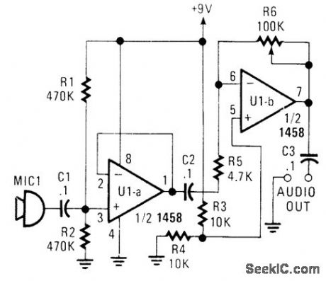
This circuit will match a crystal microphone to a device that requires a low-impedance dynamic microphone. (View)
View full Circuit Diagram | Comments | Reading(1414)
AUTOMATIC_VIDEO_SWlTCH
Published:2009/7/9 3:06:00 Author:May
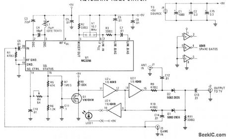
Turn on a game, computer, videodisc player, or whatever, and its output takes priority over the antenna-derived signal-the antenna is disconnected and the alternate source is fed to the monitor. When the alternate video source is no longer detected, the switch automatically reconnects the antenna. When the rf carrier is detected, a high logic output appears at pin 15 of U1-squelch status. The signal is then buffered to VMOS FET Q1. This FET can drive CMOS inverter/buffer U2, can be an open-drain output to drive a relay, or can convert to a 5 V logic level. When pin 15 of U1 becomes high, Q1 turns on, pulling pin 11 of U2e low; in turn, pin 12 becomes high. The output of U2e is fed to U2f, forcing its output, at pin 15, low. When the signal at U2 pin 12 is high, D1 is biased on, allowing the signal at J3 to flow through C14, D1, and out to J2 through C13. When the signal at J3 is removed, U1 pin 15 decreases. That decrease causes U2 pin 12 to decrease and U2 pin 15 to increase. When the signal at U2 pin 15 is high, it biases D2 on, allowing the signals at J1 to flow through C12, D2, and out to J2 through C13. (View)
View full Circuit Diagram | Comments | Reading(1114)
GENERAL_PURPOSE_POWER_SUPPLY
Published:2009/7/9 3:03:00 Author:May


The supply 6-66 can be used for supply output voltages from 1 to 35 V. The line transformer should be selected to give about 1.4 times the desired output voltage from the positive side of ftlter capacitor C1 to ground. Potentiometer R2 sets the output voltage to the desired value by adjusting the referince input.RSC is the current limit set resistor. Its value is calculated as:For example,if the maxlmum current output is to be 1 A,RSC=0.65/1.0=0.65Ω.The 1-KΩ resistor,RS,is a light-loaded resistor designed to improve the no-load stability of the supply. (View)
View full Circuit Diagram | Comments | Reading(1443)
FULL_CUP_DETECTOR_FOR_THE_BLIND
Published:2009/7/9 3:03:00 Author:May

At the heart of the Full-Cup Detector is a 555-oscillator/timer conftgured to produce a 15-Hz click, until its probe contacts are bridged, at which time its output frequency goes to about 500 Hz.
This circuit can be used by the visually handicapped to determine when a cup or bowl is full of liquid (coffee, soup, etc). U1, an NE555, produces ticks at 15 Hz. A set of probes (wire, etc.) is placed in the container at the desired level. When the liquid level contacts the probes, the frequency of clicks increases to several hundred hertz, depending on its conductivity. (View)
View full Circuit Diagram | Comments | Reading(972)
ULTRA_LOW_NOISE_MAGNETIC_PHONO_PREAMP
Published:2009/7/9 3:00:00 Author:May

This phono preamp uses an LM381/1Ain a cir-cuit that includes RIAA equalization. Adjust R7 fora voltage that is equal to half of the supply voltage(≈16.5 V). (View)
View full Circuit Diagram | Comments | Reading(1329)
RAIN_ALARM
Published:2009/7/9 3:00:00 Author:May
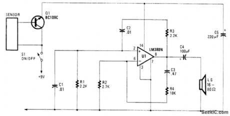
This rain sensor causes Q1 to conduct when conductive liquid (rainwater, etc.) applies bias to its base.This bias triggers LM380N oscillator and causes LS to emit a tone. (View)
View full Circuit Diagram | Comments | Reading(0)
| Pages:904/2234 At 20901902903904905906907908909910911912913914915916917918919920Under 20 |
Circuit Categories
power supply circuit
Amplifier Circuit
Basic Circuit
LED and Light Circuit
Sensor Circuit
Signal Processing
Electrical Equipment Circuit
Control Circuit
Remote Control Circuit
A/D-D/A Converter Circuit
Audio Circuit
Measuring and Test Circuit
Communication Circuit
Computer-Related Circuit
555 Circuit
Automotive Circuit
Repairing Circuit