
Circuit Diagram
Index 919
ULTRASONIC_RECEIVER
Published:2009/7/9 1:02:00 Author:May
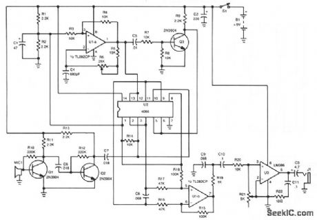
The piezo speaker, MIC1, picks up the incoming ultrasonic signal and feeds it to the base of Q1. The two-transistor booster amplifier, Q1 and Q2, raises the signal to a level that is sufficient to drive one input of this most unusual mixer circuit.Integrated circuit U2, a quad bilateral switch, functions as an extremely clean balanced-mixer circuit for the superheterodyne receiver. Integrated circuit Ula, 1/2 of a dual op amp, is connected in a variablefrequency square-wave oscillator circuit. Resistors R5, R6, and capacitor C4 determine the frequency and tuning range of the oscillator.The oscillator's square-wave output is fed along two paths. In one path, the output of U1a is input to pins 12 and 13 of U2. In the other path, the signal is fed to the base of Q3, which is configured as an inverter. The inverter outputs a signal that is 180°out-of-phase with the input signal. The inverted output of Q3 is then fed to U2 at pins 5 and 6. There, the two input signals, the ultrasonic input from MIC1 and the oscillator output, are mixed. The mixing of the ultrasonic input and the square-wave signal produces an audible product that is fed to the input of a differential amplifier, Ulb, the second half of the dual op amp, which has a voltage gain of two. The output of Ulb at pin 7 is filtered by R19 and C9 to remove the highfrequency content of the mixed signal.Only the difference frequency is important; the sum frequency, the incoming ultrasonic signal added to the oscillator frequency, is too high for the human ear to hear. The sum frequency is removed by R19 and C9 to produce a clean output signal to feed power-amplifier U3. Resistor R21 functions as the circuit's volume control.
(View)
View full Circuit Diagram | Comments | Reading(0)
Frequency_synthesizer_using_internal_time_base
Published:2009/7/20 22:45:00 Author:Jessie

Frequency synthesizer using internal time base. The counter shown is an Intersil 8240 programmable timer/counter. The output of the circuit is a positive pulse train with a pulse width equal to T and a period equal to (N+1) T, where N is the programmable count between 1 and 255. The modulus N is the total count corresponding to the counter outputs connected to the output bus. For example if pins 1, 3 and 6 are connected to the output bus the total count is N =1+4+32=37 and the period of the output waveform is equal to (N+1) T or 38T. And T=RC (courtesy Intersil, Inc.). (View)
View full Circuit Diagram | Comments | Reading(617)
1500_W_BF_AMPLIFIER
Published:2009/7/9 1:01:00 Author:May
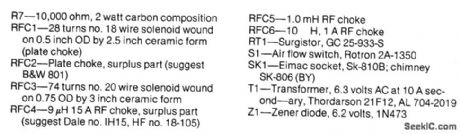
The frequency range of this amplifier is 1.8 to 54 MHz.The amount of RF drive required for full out-put is about 30 W. The grid compartment (R1, R2, RFC4,RFC5)should be shielded from the othercircuitry-especially the output circuitry. (View)
View full Circuit Diagram | Comments | Reading(583)
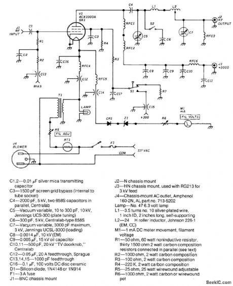
4_W_AMPLIFIER_FOR_900_MHz
Published:2009/7/9 0:56:00 Author:May
Using Wilkinson power dividers in the base and collector circuits of Q2 and Q3, two SD1853 devices are paralleled for twice the power output of the 2-W amplifier. (View)
View full Circuit Diagram | Comments | Reading(683)
5_volt_40_ampere_power_inverter_supply
Published:2009/7/20 21:34:00 Author:Jessie

5-volt 40-ampere power inverter supply (courtesy Motorola Semiconductor Products Inc.). (View)
View full Circuit Diagram | Comments | Reading(1298)
ULTRASONIC_TRANSCEIVER_1
Published:2009/7/9 0:56:00 Author:May

This ultrasonic transmit/receive circuit operates at 40 kHz. Control resistor R5 adjusts the frequency for best performance with the transducers used. (View)
View full Circuit Diagram | Comments | Reading(1462)
SERIES_REGULATION_AT_3_V
Published:2009/7/20 21:32:00 Author:Jessie
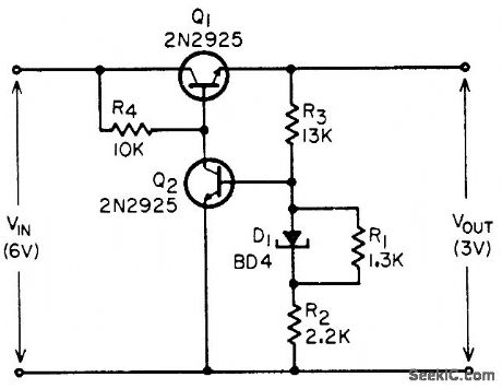
Combination of backward diode and resistor network serves as reference for regulated outputs below 6 v, for which temperature -compensated zener diodes are not available. Provides input regulation of 100:1 over 10% change in input voltage, with output impedance of 0.04 ohm. -T. P. Sylvan, Backward-Diode Power-Supply Reference Elements, EEE, 13:11, p 46-48. (View)
View full Circuit Diagram | Comments | Reading(567)
256_LEVEL_HOLD
Published:2009/7/20 21:32:00 Author:Jessie

Uses digital approximation to hold sampled analog voltage for long periods. Cascaded SN7493 ICs form 8-bit binary counter providing 256 discrete voltage levels from opamp A2, while input voltage provides varying reference to opamp A1 serving as comparator. Apply0 at reset input to clear counter for period determined by monostable IC. Counter now feeds staircase waveform to A1 through A2 until staircase reaches Vin, when counter goes high and disables counter clock. Count is then held and sampled voltage appears at output.-N. Macdonald, Digital Sample and Hold, Wireless World, May 1976, p 78. (View)
View full Circuit Diagram | Comments | Reading(1168)
7__10__15__20__25__35_watt_AF_power_amplifier_with_PNP_driver
Published:2009/7/20 21:32:00 Author:Jessie
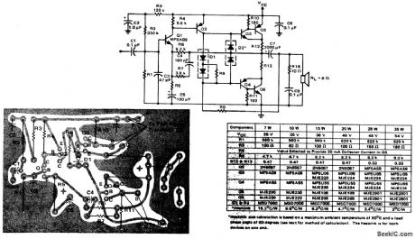
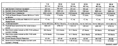
7-/10-/15-/20-/25-/35-watt AF power amplifier with PNP driver (courtesy Motorola Semiconductor Products Inc.). (View)
View full Circuit Diagram | Comments | Reading(796)
Digitally_programmed_power_supply
Published:2009/7/20 21:31:00 Author:Jessie

Digitally programmed power supply. A D/A convener with an op amp supplies voltage in accordance with a digital code (courtesy Analog Devices, Inc.). (View)
View full Circuit Diagram | Comments | Reading(634)
TIMED_SLOPE_SAMPLING
Published:2009/7/20 21:31:00 Author:Jessie

Circuit measures rate of signal change for slowly varying signals (changing less than 1 V/min) by using sample-and-hold circuit to store instantaneous sample.After compatible time interval, sample is com-pared with new input current value; difference is then the desired slope. One limitation is that offset errors added to stored signal near zero voltage can cause large errors in the derivative. Circuit is highly sensitive to noise spikes during sampling.-R. E. Bober, This Derivative Circuit Handles Slowly Varying Signals, EDN Magazine, Jan. 20, 1976, p 82. (View)
View full Circuit Diagram | Comments | Reading(655)
OPTOISOLATOR
Published:2009/7/9 0:54:00 Author:May

The circuit protects a solid-state relay from overloads. The circuit limits current, automatically discon-nects the load after detecting a short circuit, and develops a fault-condition output signal.In normal operation, the controlling ptP sets the flip-flop, IC1, which turns on transistor Q1. When Q1 turns on, current flows through the solid-state relay's input, thus activating the relay.If an overcurrent or fault condition occurs, the excessive load current flowing through the relay develops enough potential across sense resistor R5 to turn on one of the optoisolators, IC4A or IC4B. The optoisolator's output transistor diverts current around the solid-state relay's input, which limits the cur-rent that the relay's output can pass.If the overload is severe enough, the optoisolator pulls the input of the Schmitt trigger above its threshold, thus clearing the flip-flop and turning off the solid-state relay. R2 has two functions: It keeps the input of the Schmitt trigger below 5 V max. to prevent latchup, and it forms an RC filter in conjunction with C1. The RC filter prevents spurious triggering of the Schmitt trigger. You can use the output of the flip-flop to signal overload conditions to the controlling μP. (View)
View full Circuit Diagram | Comments | Reading(2190)
120_KHz_500_W_INDUCTION_HEATER
Published:2009/7/9 0:52:00 Author:May

Variable width pulses with fast rise times are provided by U1, and MC34060 operating at 120 kHz, the optimum frequency for heating aluminum alloy containers. The pulse width is modulated by sensing the temperature of the target with a thermistor, using its negative temperature coefficient to change pulse duration. The MC34060 produces output pulses that are accoupled to push-pull MJE200 transistors Q1 and Q2. This IC provides the current needed to ensure fast switching for MTM15N45 TMOS power FET Q3.The estimated efficiency is 80%, based on switching losses and an RON of 0.4 Ω (max). The MTM15N45, with maximum ratings of 15 A and 450 V, was chosen because the induction heater might be operated from either 115 or 220 V sources. A modest heatsink is required because 100 W is dissipated in the power FETs at a full output power of 500 W. (View)
View full Circuit Diagram | Comments | Reading(6100)
THYRATRON_REGULATOR
Published:2009/7/20 21:30:00 Author:Jessie

Output of 12 to 16 v is regulated within 1% for loads of 6 to 22 ma. Since 2D21 can handle 100 ma continuously, circuit is easily modified to regulate higher current values.-W. D. Fryer, Thyratron Regulates Supply, Electronics, 31: 25, p 88. (View)
View full Circuit Diagram | Comments | Reading(732)
SOLID_STATE_RELAY
Published:2009/7/9 0:49:00 Author:May
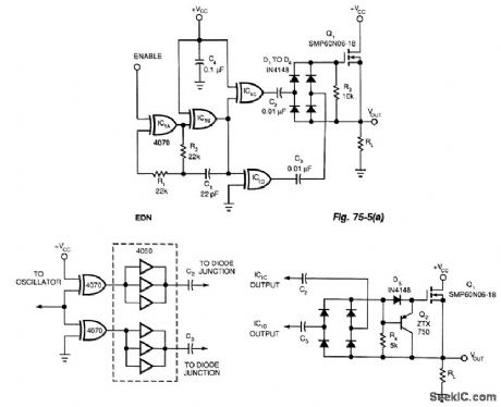
A power MOSFET and a quad exclusive-OR oscillator makes an effective solid-state relay. Figure 75-S(a)'s capacitively isolated drive circuit provides gate drive to turn on the n-channel device. This con-sists of a gated oscillator (IC1A and IC1B running at 500 kHz, set by R1, R2, and C1).The diode bridge (D1 through D4) rectifies the charge transferred through C2 and C3. When you dis-able the oscillator, R3 discharges the stored gate charge, thereby turning off the MOSFET. R3 needs to allow fast turn-off times without loading the gate's enhancement voltage. A value of 10-k0 is sufficient to produce a turn-off time of 800 ;ts with an 18-mΩ SMP60N06-18 MOSFET. The measured turn-on time is 150 μs.You can reduce the turn-off time to 100 pts by using a pnp transistor as a diode-steering emitter-fol-lower in the MOSFET gate circuit (Fig. 75-5(b)). Adding a hex buffer to Fig. 75-5A's circuit increases the drive capability of the complementary outputs (Fig. 75-5(c)). (View)
View full Circuit Diagram | Comments | Reading(2785)
Direct_line_operated_power_supply_for_line_operated_servo_amplifier
Published:2009/7/20 21:30:00 Author:Jessie
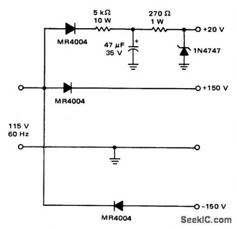
Direct-line-operated power supply for line-operated servo amplifier (courtesy Motorola Semiconductor Products Inc.). (View)
View full Circuit Diagram | Comments | Reading(499)
DELAY_OFF_RELAY_CIRCUIT
Published:2009/7/9 0:45:00 Author:May
When voltage is applied to the capacitor, it charges. While it's charging, the relay remains latched. When the charging current falls below the level needed to hold the relay down, the relay unlatches. The higher the value of the capacitor, the longer the relay will remain latched. (View)
View full Circuit Diagram | Comments | Reading(938)
NONINVERTING_SAMPLE_AND_HOLD_1
Published:2009/7/20 21:29:00 Author:Jessie

DG181 JFET analog switch provides best combination of settling speed and inherent charge transfer accuracy for 2N5545 FET-input opamp for high-speed sample-and-hold applications.- Analog Switches and Their Applications, Siliconix, Santa Clara, CA, 1976, p 7-60. (View)
View full Circuit Diagram | Comments | Reading(579)
LOW_CONSUMPTION_MONOSTABLE_RELAY
Published:2009/7/9 0:44:00 Author:May
A monostable relay has two states: operative when a large enough current flows through its coil and quiescent when no current flows. A relay contact that assumes a certain position after the supply voltage has been switched on is required in many applications. Of course, many relays operate in that manner.However, most of these relays require an energizing current of 50 mA or more and that normally pre-cludes a battery supply. The circuit presented here, which uses a bistable relay, can solve that problem.The contact of a bistable relay normally remains in the position it is in after the supply is switched off. This circuit, however, makes the bistable relay behave like a monostable type, at a modest current.When the supply voltage is switched on, C1 charges via D1 and the relay coil. The current then flow-ing through the coil causes the relay contact to assume one of two positions. The forward drop across D1 ensures that the base of T1 (in this condition) is more positive than its emitter so that T1, and thus T2, is switched off.When the supply voltage is switched off, the emitter of T1 is connected to the positive terminal of C1, while the base is connected to the negative terminal of the capacitor via R1 and the relay coil. This results in T1, and thus T2, switching on so that C1 discharges via T4 and the relay. The current flows through the relay coil, then ftows in an opposite direction and this causes the contact to change oven The bistable relay thus behaves exactly as a monostable with the advantage, however, that the opera-tional current is determined by R1, which amounts to only 130 μA. To ensure reliable operation, the rating of the relay coil should be 65 to 75% of the supply voltage. In the prototype, a 9-V relay was used with a battery supply voltage of 12 V. (View)
View full Circuit Diagram | Comments | Reading(1796)
VOLTAGE_SPLITTER_REGULATOR
Published:2009/7/20 21:29:00 Author:Jessie
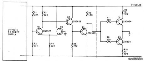
Provides regulated +12 and -12 v from 24-v supply Negative feedback loop permits circuit to furnish unbalanced currents up to 700 ma in either direction without changing output voltages more than 10 my.-J. M. Kasson, Voltage Splitter Balances Floating Power Supply, Electronics, 39:6, p 96. (View)
View full Circuit Diagram | Comments | Reading(1471)
| Pages:919/2234 At 20901902903904905906907908909910911912913914915916917918919920Under 20 |
Circuit Categories
power supply circuit
Amplifier Circuit
Basic Circuit
LED and Light Circuit
Sensor Circuit
Signal Processing
Electrical Equipment Circuit
Control Circuit
Remote Control Circuit
A/D-D/A Converter Circuit
Audio Circuit
Measuring and Test Circuit
Communication Circuit
Computer-Related Circuit
555 Circuit
Automotive Circuit
Repairing Circuit