
About SeekIC | Services | Payment | Advertisements service | Contact Us | Links
© 2008-2012 SeekIC.com Corp.All Rights Reserved.

Published:2009/7/20 6:51:00 Author:Jessie

Balanced modulator using an MC1545G wide-band amplifier (courtesy Motorola Semiconductor Products Inc.). (View)
View full Circuit Diagram | Comments | Reading(973)
Published:2009/7/9 4:12:00 Author:May

The output frequency of the VCO, U1, vanes inversely with the input voltage. With a 1-V input, the oscillator output frequency is about 1500 Hz; with a 5-V input, the output frequency drops to around 300 Hz. The output frequency range of U1 can be altered by varying the values of C1, R2, and R3. Increasing the value of any those three components will lower the oscillator frequency, and decreasing any of those values will raise the frequency. Output-waveform symmetry suffers since the frequency varies from one extreme to the other. At the highest frequency, the waveform is almost equally divided. But when the frequency drops, the output of the circuit turns into a narrow pulse. If a symmetrical waveform is required, add the second IC, U2, half of a 7473P dual TTL J-K flip-flop, to the oscillator circuit. The signal frequency output by U2 is 1/2 of the input. (View)
View full Circuit Diagram | Comments | Reading(911)
Published:2009/7/20 6:50:00 Author:Jessie

250 MHz BF to 50 MHz IF mixer using a 2N3308 transistor. The external local oscillator injection frequency is 300 MHz,The outputof the 2N3308 is tuned to the difference between the two signals (courtesy Motorola semiconductor Products Inc.). (View)
View full Circuit Diagram | Comments | Reading(868)
Published:2009/7/20 6:49:00 Author:Jessie
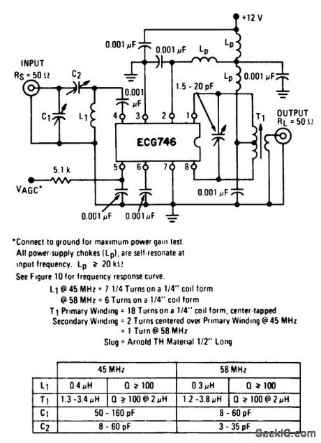
BF amplifier for 45 MHz or 58 MHz. See table for component selection (courtesy GTE Sylvania Incorporated). (View)
View full Circuit Diagram | Comments | Reading(925)
Published:2009/7/9 4:12:00 Author:May

This circuit uses an RCA CA3162E (IC2) A/D converter. This converter has 12-bit output (BCD) which is sent to display decoder driver IC1. +5 V is obtained from IC1. R17 adjusts to 0 and R11 should be set to produce correct calibration of gauge unit. Displays are common cathode types. No limiting resistors are necessary because the output drivers are constant current. R15 and R16 sample the applied voltage (usually 8 to 18 V). LED1 is used to illuminate the gauge legend (Volts, Temp, etc.). (View)
View full Circuit Diagram | Comments | Reading(4203)
Published:2009/7/9 4:12:00 Author:May

This circuit is basically the classic bucking regulator, except it uses a TMOS N-channel power FET for the chopper and creates its own supply for the gate control.The unique aspect of this circuit is how it generates a separate supply for the gate circuit, which must be greater than VDD. When power is applied, C2 charges, through D2, to + 12 V. At this time, Q1 is off and the voltage at point A is just below zero. When the pulse-modulated signal is applied, the optoisolator transistors, Q2 and Q3, supply a signal to Q1 that turns it on. The voltage at point A then goes to VDD, C2 back-biases D2, and the voltage at point B becomes 12 V above VDD.After Q1 is turned on, current starts to flow through L1 into C1, increasing until Q1 turns off. The current still wants to flow through L1, so the voltage at point A moves toward negative infinity, but is clamped by D1 to just below zero. Current flows less and less into C1, until Q1 turns on again. Q2 and Q3 drive Q1's gate between the voltages at point A and B, which is always a 12 V swing, so %g max. is never exceeded. For proper operation, the 12-V supply has to be established before the pulse-width modulator signal is applied. (View)
View full Circuit Diagram | Comments | Reading(766)
Published:2009/7/20 6:48:00 Author:Jessie
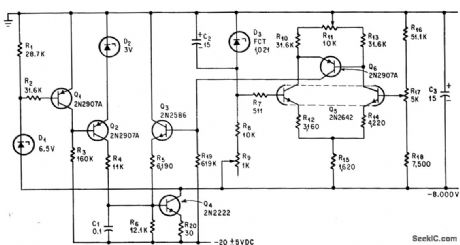
Output voltage is held within 0.1% despite 5-v variations in 20-v input to regulator that itself consumes only 1.5 ma. Differential amplifier Q5 acts as voltage comparator, with zener diode D3 as reference.-A. Dargis, A High Performance Voltage Regulator, Electronics, 37:13, p 75. (View)
View full Circuit Diagram | Comments | Reading(654)
Published:2009/7/9 4:11:00 Author:May


Suitablefor use as active probefor CRO,as electrometer,and for instrumentation applications Combination of unipolar and bipolar transistors gives desirable amplifying features of each solid-state device.-I. M. Gottlieb,A New Look at Solid-State Amplifiers,Ham Radio,Feb 1976,p 16一19.
(View)
View full Circuit Diagram | Comments | Reading(972)
Published:2009/7/20 6:46:00 Author:Jessie
Used when output can be less than zener voltage.- Zener Diode Handbook, International Rectifier Corp., 1960, p 55. (View)
View full Circuit Diagram | Comments | Reading(714)
Published:2009/7/9 4:10:00 Author:May

Using an intersil ICL 7106 A/D converter chip and an LED display module, this gauge uses a Sensym Corp. pressure transducer SX100pn (100 psi full scale) in a Wheatstone bridge configuration to drive an op amp (ICla, b, c) translator circuit that supplies a dc voltage to IC2 that is proportional to pressure. R6 sets the gain of ICIA (full-scale sensitivity) and R16 supplies a zero adjustment. IC3 provides regulated + 5 V to power the circuit. (View)
View full Circuit Diagram | Comments | Reading(3634)
Published:2009/7/9 4:10:00 Author:May

Germanium transistor Q1 is used as a noise generator in the audio range. U1 acts as a high-gain ampli-fter. Q1 is not critical; most germanium transistors appear to be satisfactory. A germanium diode can also be substituted. This circuit is mainly used for sound effects and noise experiments. It is not flat over the audio range because of unpredictable effects in Q1, but it should be useful where high precision is not necessary. (View)
View full Circuit Diagram | Comments | Reading(0)
Published:2009/7/9 4:09:00 Author:May
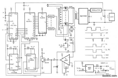
One of the control circuit's triacs selects the tap on main transformer T1, which provides the proper, preregulated voltage to the secondary regulator. T2 and its associated components comprise the second-ary regulator.The ADO 0804, IC1, digitizes a voltage-feedback signal from the secondary regulator's output. The MC1415 demultiplexer, IC2, decodes the digitizer's output. IC2, in turn, drives T1's optoisolated triacs via the 74LS240 driver chip, IC3, and associated optoisolators.Transformer T3 samples the circuit's current output. The auxiliary, 12 V winding on T1 ensures no-load starting. The combination of op amp IC5 and the inverting transistor, Q1, square this current signal. The output of Q1 is the CLK signal, which triggers one-half of the one shot, IC4A, to begin the circuit's A/D conversion. The one shots' periods are set to time out within 1/2 cycle of the ac input.Upon completion of its A/D conversion, IC1's INTR output triggers the other half of the one shot, IC4B, which enables the converter's data outputs. The rising edge of the CLK signal resets the one shot and latches the new conversion value into IC2. The latch, associated driver, and optoisolator trigger a selected triac according to the latest value of the voltage-feedback signal, VO. (View)
View full Circuit Diagram | Comments | Reading(1275)
Published:2009/7/9 4:08:00 Author:May

At startup, the voltage in the trigger input at pin 2 is less than the trigger level voltage, 1/3 VDD, causing the timer to be triggered via pin 2. The output of the timer at pin 3 becomes high, allowing capacitor Ct to charge very rapidly through diode D1 and resistor R1.When capacitor Ct charges to the upper threshold voltage 2/3 VDD, the flip-flop is reset, the output at pin 3 decreases, and capacitor Ct discharges through the current mirror, TL011. When the voltage at pin 2 reaches 1/3 VDD, the lower threshold or trigger level, the timer triggers again and the cycle is repeated. (View)
View full Circuit Diagram | Comments | Reading(1260)
Published:2009/7/9 4:08:00 Author:May
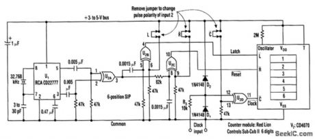
This counter makes direct readout of frequency-generating equipment very easy when a 1-Hz time-base is added to latch, reset, and the count signal is conditioned. This design has the flexibility to select either polarity.
By differentiating, inverting, and ORing the clock pulses in XOR gate U2A, a stream of 1-Hz, positive, 200-μs pulses is generated. For latching, the 1-Hz stream is again differentiated in U2B, input 1 to supply a 50-μs pulse. Though U2B's output goes from high to low, it can be reversed, by making input 2 low.
Because the reset pulse must occur after the latch signal, the 1-Hz stream from U2A is delayed 100 μs at U2C input 1. The output-pulse polarity is determined by making U2C's input 2 either high or low. (View)
View full Circuit Diagram | Comments | Reading(736)
Published:2009/7/9 4:07:00 Author:May

This circuit for starting arc jets and controlling them in steady operation is capable of high power efficiency and can be constructed in a lightweight form. The design comprises a pulse-width-modulated power converter, which is configured in a closed control loop for fast current control. The series averaging inductor maintains nearly constant current during rapid voltage changes, and thereby allows time for the fastresponse regulator to adjust its pulse width to accommodate load-voltage changes. The output averaging inductor doubles as the high-voltage pulse transformer for ignition. The starting circuit operates according to the same principle as that of an automobile ignition coil. When the current is interrupted by a transistor switch, the inductor magnetic field collapses, and a high-voltage pulse is produced. The pulse is initiated every 0.25 second until arc current is detected, then the pulser is automatically turned off. (View)
View full Circuit Diagram | Comments | Reading(1466)
Published:2009/7/9 4:04:00 Author:May
View full Circuit Diagram | Comments | Reading(834)
Published:2009/7/20 6:45:00 Author:Jessie
30 MHz IF strip for microwave or radar receivers using three ECG703A ICs (courtesy GTE Sylvania Incorporated). (View)
View full Circuit Diagram | Comments | Reading(1029)
Published:2009/7/9 4:03:00 Author:May

The internal zener on pin 15 of the 4046B supplies a stable voltage to the 3140lC op amp. This ampli-fter modulates the 4046B VCO. The amplifier gain is about 20x (26 dB voltage). The VCO produces a 220-kHz carrier that is FM modulated. C3 can be changed to vary this frequency. (View)
View full Circuit Diagram | Comments | Reading(1449)
Published:2009/7/9 4:02:00 Author:May
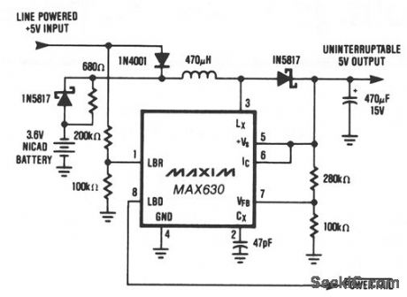
This circuit provides a continuous supply of regulated + 5 V, with automatic switch-over between line power and battery backup. When the line-powered input voltage is a +5 V, it provides 4.4 V to the MAX630 and trickle charges the battery. If the line-powered input falls below the battery voltage, the 3.6 V battery supplies power to the MAX630, which boosts the battery voltage up to + 5 V, thus maintain-ing a continuous supply to the uninterruptable + 5 V bus. Since the + 5 V output is always supplied through the MAX630, there are no power spikes or glitches during power transfer. The MAX630's low-battery detector monitors the line-powered +5 V, and the LBD output can be used to shut down unnecessary sections of the system during power failures. Alternatively, the low-battery detector could monitor the NiCad battery voltage and provide warning of power loss when the battery is nearly discharged. Unlike battery backup systems that use 9-V batteries, this circuit does not need + 12 or + 15 V to recharge the battery. Consequently, it can be used to provide + 5 V backup on modules or circuit cards which only have 5 V available. (View)
View full Circuit Diagram | Comments | Reading(643)
Published:2009/7/20 6:45:00 Author:Jessie
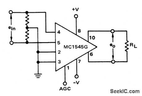
Wide-band differential amplifier with AGO using an MC1545G (courtesyMotorola Semiconductor Products Inc.). (View)
View full Circuit Diagram | Comments | Reading(851)
| Pages:900/2234 At 20881882883884885886887888889890891892893894895896897898899900Under 20 |
Response in 12 hours
© 2008-2012 SeekIC.com Corp.All Rights Reserved.