
Circuit Diagram
Index 887
SUBAUDIBLE_TONE_ENCODER
Published:2009/7/20 4:50:00 Author:Jessie

Simple crystal-controlled oscillator drives CD4020 CM0S divider to give output frequency below normal voice range, for providing tone access to repeater. With 1.120-MHz crystal and division ratio of 8192, output is 136.7 Hz. Output circuit is RC filter that converts square wave to triangle, with pot setting level. Article tells how to choose crystals for other output frequencies and division ratios.-C. Haines, Jr., Go Tone for Ten, 73 Magazine, Dec. 1976, p 22-23. (View)
View full Circuit Diagram | Comments | Reading(3792)
IR_RECEIVERI
Published:2009/7/9 5:39:00 Author:May

This receiver is built around a μPC1373 IR remote-control preamplifier, a sensitive 30-to-40 kHz tuned detector, an autoniatic gain control, a peak detector, and an output waveshaping buffer. The demod-ulated signal from the preamp stage is sent to IC4A, a 74C14 Schmitt trigger. The squared-up 1 500-Hz signal is then sent to the clock input of IC5A, half of a 4013 dual D flip-flop. That 750-Hz signal is clipped to approximately 0.7-V p-p by diodes D3 and D4. The clipped signal is then fed to IC6, a 567 tone decoder. The output of that IC goes low whenever the frequency of the signal fed to it is within the lock range of its internal VCO.
When IC6 detects a signal of the proper frequency, pin 8 goes low. The output signal is fed through another Schmitt trigger (IC4B), which drives another D flip-flop, IC5B. Schmitt trigger IC4B also drives IC4C, which in turn drives LED4, SIGNAL, which fights up whenever a signal is received. The Q output of IC5B drives two parallel-connected inverters. IC4C and IC4F turn transistor Q2 on when Q goes low. That transistor energizes the relay; its contacts switch the controlled device on and off. (View)
View full Circuit Diagram | Comments | Reading(732)
14_bit_sign_magnitude_binary_convener_using_an_ADC1105
Published:2009/7/20 4:50:00 Author:Jessie

14-bit sign-magnitude binary convener using an ADC1105 (courtesy Analog Devices, Inc.). (View)
View full Circuit Diagram | Comments | Reading(881)
TRANSMITTER_OUTPUT_INDICATOR
Published:2009/7/9 5:38:00 Author:May

Relative power can be indicated with this simple circuit.Adjust the 365-pF variable capacitor fordesired lamp brightness. (View)
View full Circuit Diagram | Comments | Reading(762)
F_V_convener_controlling_and_monitoring_motor_speed_in_a_closed_loop_system
Published:2009/7/20 4:49:00 Author:Jessie

F/V convener controlling and monitoring motor speed in a closed loop system.The F/V convener is a 451/453 10/100 kHz F/V convener with a +10-volt full scale output (courtesy Analog Devices, Inc.). (View)
View full Circuit Diagram | Comments | Reading(856)
SOUND_SENSOR
Published:2009/7/9 5:37:00 Author:May

By using a microphone,high-gain amplifier(Fig.37-10(b)),and detector-relay driver(Fig.37-10(a)asound-detecting alarm system can be constructed.If you want a latching setup,make the dotted connection to the relay shown h Fig.37-10(a) (View)
View full Circuit Diagram | Comments | Reading(1730)
COINCIDENT_SLICER_PHASEMETER
Published:2009/7/20 4:49:00 Author:Jessie

Cathode-coupled limiters convert input signals to square waves and feed them to coincident slicer. Self-adjustment of limiters and use of coincident slicer to drive direct-reading phase-meter give good accuracy and stability for input-signal fluctuations from 0.3 to 70 V and supply voltages from 94 to 135 V, with absolute accuracy of 1° and relative accuracy of 0.25°.-Y. P. Yu, Coincident Slicer Measures Phase Directly, Electronics, 31:37, p 99-101. (View)
View full Circuit Diagram | Comments | Reading(636)
PORTABLE_NICAD_CHARGER
Published:2009/7/9 5:36:00 Author:May
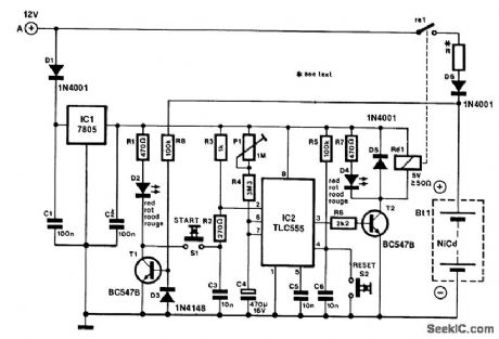
The portable charger is intended primarily to give model enthusiasts the opportunity of charging their Nicad batteries from a car battery out in the open. The supply voltage for the circuit is regulated by IC1.
When the circuit is connected to the car battery, D2 lights only if the Nicad to be charged has been connected with correct polarity. For that purpose, the + terminal of the Nicad battery is connected to the base of T1 via R8. Because even a discharged battery provides some voltage, T1 is switched on and D2 lights.
Only if the polarity is correct will the pressing of the start switch, S1, have any effect. If so, the collec-tor voltage of T1 is virtually zero so that monostable IC2 is triggered by S1. The output, pin 3, of this CMOS timer then becomes high, T2 is switched on and relay Re1 is energized. Charging of the Nicad battery, via R5 and D6, then begins and charging indicator D4 lights. During the charging, C4 is charged slowly via P1 and R4. The.value of these components determines the mono time of IC2 and thus the charging period of the Nicad battery. With values as shown in the diagram, that period can be set with P1 to between 26 and 33 min. Notice that this time is affected by the leakage current of C4; use a good-quality capacitor here. The charging can be interrupted with reset switch S2.
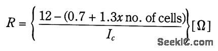
The charging current through the Nicad battery is determined by the value of R, which can be calcu-lated:
IC is the charging current, which is here because the chosen charging period is twice the nominal value of the capacity of the Nicad battery. Resistor R must be able to dissipate a power of IC2RW. Finally, make sure that the Nicad battery is suitable for fast charging; never charge for longer than half an hour! (View)
View full Circuit Diagram | Comments | Reading(764)
PREFERRED_150_V_D_C_REGULATOR
Published:2009/7/20 4:49:00 Author:Jessie

Provides either polarity of output with l% regulation, from minimum of 190 v d-c input. Maximum load current is 100 ma per series tube. C4 is minimum of 4 mfd.-NBS, Hand-book Preferred Circuits Navy Aeronautical Electronic Equipment, Vol. 1, Electron Tube Circuits, 1963, PC 4, p 4-2. (View)
View full Circuit Diagram | Comments | Reading(707)
8_bit_D_A_convener_with_voltage_regulator
Published:2009/7/20 4:49:00 Author:Jessie

8-bit D/A convener with voltage regulator (courtesy Motorola Semiconductor Products Inc.). (View)
View full Circuit Diagram | Comments | Reading(884)
CONTROL_TONE_GENERATOR
Published:2009/7/20 4:48:00 Author:Jessie

Uses NE566V PLL as tone generator, directly connected to microphone input of transmitter for activating loudspeaker in receiver being called. Operation is similar to that of paging units using selective call tones output level of PLL is adjusted so tone is same amplitude as voice.-K, Wyatt, Private Call System for VHF FM,Ham Radio, Sept,1977,p62-64 (View)
View full Circuit Diagram | Comments | Reading(708)
The FET therapeutic apparatus
Published:2011/7/21 20:30:00 Author:qqtang | Keyword: FET, therapeutic apparatus

The working principle of the circuitThe FET therapeutic apparatus is simple, which consists of the fuse FU, power supply transformer T, power supply switch S1, voltage regulation switch S2, current limit resistor R, power supply indicator LED VL and FET band, see as figure 9-26.
When the power is on, its indicator VL is glowing. At the same time, there generates a inducting voltage on the secondary coil of the transformer T. The core voltage is added on the FET band, which generates the alternating field, eddy field and infrared rays. (View)
View full Circuit Diagram | Comments | Reading(548)
1_Hz_TO_10_MHz_VOLTAGE_TO_FREQUENCY_CONVERTER
Published:2009/7/9 5:35:00 Author:May

View full Circuit Diagram | Comments | Reading(951)
LINEAR_LIGHT_METER
Published:2009/7/9 5:35:00 Author:May

Uses Radio Shack 276-115 selenium solar cell or equivalent photocell with high-gain RS741C opamp to drive meter.Sensitivity is sufficient to detect individual stars at night without magnifying lens if photocell is shielded from ambient light with length of cardboard tubing. Increasing value of R1 increases gain and sensitivity of circuit. R2 sets meter needle to zero when sensor is dark.- F. M Mints, Integrated Circuit Projects, Vol. 4, Radio Shack, Fort Worth, TX, 1977, 2nd Ed., p 45-53. (View)
View full Circuit Diagram | Comments | Reading(1263)
General_purpose_voltage_preamplifier
Published:2009/7/20 4:42:00 Author:Jessie

General-purpose voltage preamplifier. Typical voltage gain is 35.5 dB. Input resistance is 120K. The EGG1103 is a 7-pin module (courtesy GTF Sylvania). (View)
View full Circuit Diagram | Comments | Reading(929)
PRESERVED_INPUT_VOLTAGE_TO_FREQUENCY_CONVERTER
Published:2009/7/9 5:32:00 Author:May

|The input voltage, V1, causes C1 to charge and produce a ramp voltage at the output of the 741 op amp. Diodes D1 and D2 are four-layer devices. When the voltage across C1 reaches the breakover voltage of either diode, the diode conducts to discharge C1 rapidly and the op amp output goes abruptly to zero. This rapid discharge action applies a narrow pulse to G1 and G2. Positive discharge pulses produced by a positive V1 are coupled to the output only through G1, while negative pulses are coupled only through G2.Because of the forward breakover current of diodes D1 and D2, the circuit won't operate below a minimum input voltage. An increase of R1 increases this minimum voltage and reduces the circuit's dynamic range. The minimum input voltage with R1 at 1 KΩ is in the range of 10 to 50 mV. This input dead zone, when input signal V1 is near zero is desirable in applications that require a signal to exceed a certain level before an output is generated. (View)
View full Circuit Diagram | Comments | Reading(561)
ON_INDICATOR
Published:2009/7/9 5:32:00 Author:May

Battery-operated equipment can work on one set of batteries for a long time nowadays. However, if it is left on inadvertently, that long time is over very quickly. Moreover, flat (dead) batteries are always found at the wrong moment. The circuit proposed here is a sort of aide-memoire. Every two minutes, it emits 5 to 10 pips to indicate that the equipment is still switched on.
Basically, the circuit consists of three rectangle-wave generators and an inverter. The first of the gen-erators is formed by N1 and provides a signal with a period of about two minutes and a pulse duration of around 10 seconds. During those 10 seconds, the second generator starts operating in a one-second rhythm. Thus, N2 outputs 10 pulses every 2 minutes. That output is inverted so that N4, like N2, can only be enabled during the 10-second pulse train from N1. The difference is that during those 10 seconds, N4 is enabled and inhibited 10 times; this is what causes the pips.
Do not take the times and number of pulses too literally, because wide variances are between ICs from different manufacturers. On the other hand, component values are not critical, so it is fairly easy to adapt the circuit to personal taste or requirements. The buzzer can be a standard Toko type or equivalent.The current drawn by the circuit is negligible. (View)
View full Circuit Diagram | Comments | Reading(775)
Multiplying_D_A_convener_using_a_Datel_DAC_MC8B_16_pin_DIP
Published:2009/7/20 4:41:00 Author:Jessie

Multiplying D/A convener using a Datel DAC-MC8B 16-pin DIP. Pin functions of the DAC-MC8B as follows: pin 1, ground; pin 2, logic select; pin 3, reset; pin 4, strobe; pin 5, bit8(LSB); pin 6, bit7; pin7, bit6; pin8, +VCC; pin 9, bit5; pin 10, bit 4; pin 11, bit3;pin 12, bit2; pin 13, bit 1(MSB); pin 14, analog output; pin 15,VREF input; pin 16, VREF output (courtesy Datel Systems, Inc.). (View)
View full Circuit Diagram | Comments | Reading(792)
MAINS_FAILURE_INDICATOR
Published:2009/7/9 5:30:00 Author:May

When the mains voltage is present at the input terminals, the transistor in the optocoupler is on, T1 is off, and silicon-controlled rectifier Th1 is in the conducting state. Because both terminals of the piezoelec-tric buzzer are then at the same potential, the buzzer is inactive. If the mains voltage drops out, transistor T1 conducts and causes one of the terminals of the buzzer to be connected to earth; the thyristor remains in the conducting state. In this situation, a large enough potential difference is across both the buzzer and D5 to cause these elements to indicate the mains failure-both audibly and visibly.
When the mains is restored, the circuit returns to its original state. A touch on the reset button then interrupts the current through the SCR so that the thyristor goes into the blocking state, and the other terminal of the buzzer is connected to ground.
The unit is powered by a 9-V battery and draws a quiescent current of 1.7-2.5 mA. It is important for the enclosure to be well-insulated.
If by accident the circuit to the optocoupler and R2 is broken, electrolytic capacitor C2 might be dam-aged because it will be charged well above its 25-V rating. Secondly, where a plug is used for the mains connection, it is advisable to solder a 1-MΩ resistor across C1 so that this capacitor does not retain its charge after the plug is removed from the mains socket. (View)
View full Circuit Diagram | Comments | Reading(2644)
PHASE_CONTROLLED_D_C_SUPPLY
Published:2009/7/20 4:41:00 Author:Jessie

Uses scr's in single-phase center-tap phase-controlled rectifier. D-c voltage across load can be adjusted steplessly from zero to maximum with R7. Single ujt Q1 develops gate signal to fire both scr's on alternate half-cycles.- Silicon Controlled Rectifier Manual, Third Edition, General Electric Co., 1964, p 140. (View)
View full Circuit Diagram | Comments | Reading(1155)
| Pages:887/2234 At 20881882883884885886887888889890891892893894895896897898899900Under 20 |
Circuit Categories
power supply circuit
Amplifier Circuit
Basic Circuit
LED and Light Circuit
Sensor Circuit
Signal Processing
Electrical Equipment Circuit
Control Circuit
Remote Control Circuit
A/D-D/A Converter Circuit
Audio Circuit
Measuring and Test Circuit
Communication Circuit
Computer-Related Circuit
555 Circuit
Automotive Circuit
Repairing Circuit