
Circuit Diagram
Index 895
58_watt_AF_power_amplifier_for_automotive_applications
Published:2009/7/20 5:20:00 Author:Jessie
5.8-watt AF power amplifier for automotive applications. This circuit is ideal for car stereo or car radio outputs. In addition it can be employed for a CB modulator circuit. Recommended supply voltage is 13.2 volts. Input resistance is 40K. Voltage gain ranges between 52 and 58 dB (courtesy GTE Sylvania Incorporated). (View)
View full Circuit Diagram | Comments | Reading(547)
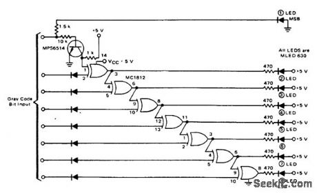
Serial_gray_to_binary_converter_above
Published:2009/7/20 5:20:00 Author:Jessie

Serial gray-to-binary converter above (courtesy Motorola Semiconductor Products Inc.). (View)
View full Circuit Diagram | Comments | Reading(909)
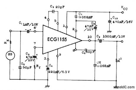
500_mW_AF_power_amplifier_for_a_20_ohm_speaker
Published:2009/7/20 5:19:00 Author:Jessie

500 mW AF power amplifier for a 20-ohm speaker. Frequency response is from 70 hertz to 20 kilohertz. The ECG1016 is a thin-film hybrid module. The AF driver transistor is standard and can be purchased en Radio Shack (courtesy GTE Sylvania Incorporated). (View)
View full Circuit Diagram | Comments | Reading(694)
8_bit_A_D_converter_using_an_ADC_MC8B_16_pin_DIP
Published:2009/7/20 5:18:00 Author:Jessie

8-bit A/D converter using an ADC-MC8B 16-pin DIP. Pin functions of the Datel ADC-MC8B chip are as follows: pin 1, ground; pin 2, logic select; pin 3, reset; pin 4, strobe; pin5, bit8 (LSB); pin6, bit7; pin7, bit6;pin8, +VCC; pin 9, bit 5; pin 10, bit4; pin 11, bit3; pin 12, bit2; pin 13, bit 1(MSB); pin 14, analog out; pin 15,VREF input; pin 16, VREF output. To calibrate, apply continous start commands to the start input. For the zero adjustment ground the analog input and vary the zero adjust pot until the LSB flickers between one and zero with all other inputs at logic zero. For the gain adjustment apply FS-1/2 LSB to the analog input and vary the gain adjust pot until LSB flickers between one and zero with all other bits at logic one (courtesy Datel Systems, Inc.). (View)
View full Circuit Diagram | Comments | Reading(1274)
PULSE_CHAIN_PHASEMETER
Published:2009/7/20 5:18:00 Author:Jessie

Measures phase difference as small as 0.005 deg between pulses of two nearly coincident pulse chains using electronic switch, mvbr phase detector, and diode synchronous detector. Output shows both sign and magnitude of phase angle between two corresponding pulses in pulse chains.-F. Vrataric, Jr., Electronic Switching in Phase Measurement, Electronics, 32:23, p 60-61. (View)
View full Circuit Diagram | Comments | Reading(2082)
8_bit_successive_approximation_A_D_converter
Published:2009/7/20 5:17:00 Author:Jessie

8-bit successive-approximation A/D converter (courtesy Motorola Semiconductor Products Inc.). (View)
View full Circuit Diagram | Comments | Reading(2390)
75_watt_AF_power_amplifier_with_low_transient_intermodulation_distortion
Published:2009/7/20 5:16:00 Author:Jessie


75-watt AF power amplifier with low-transient-intermodulation distortion (courtesy Fairchild Semiconductor). (View)
View full Circuit Diagram | Comments | Reading(1640)
High_speed_8_bit_successive_approximation_A_D_convener
Published:2009/7/20 5:16:00 Author:Jessie

High-speed 8-bit successive-approximation A/D convener (courtesy Motorola Semiconductor Products Inc.). (View)
View full Circuit Diagram | Comments | Reading(798)
D_A_convener_with_output_buffer
Published:2009/7/20 5:14:00 Author:Jessie

D/A convener with output buffer. VOUT is directly proportional to the digital input.R2 should be less than or equal to 650K to assure good temperature compensation. Metal film 1% resistors and 100 PPM/℃ trimmers are recommended. For fast settling time use a Datel AM-452 buffer. To calibrate apply continuous start commands to the start input (pin 3). Set all bits to logic zero and vary the zero adjust pot until VOUT is zero. Set all bits to logic one and vary the gain adjust pot until VOUT is equal to the nominal FS-1 LSB, where LSB is equal to FSR/256 (courtesy Datel Systems, Inc.). (View)
View full Circuit Diagram | Comments | Reading(797)
Cyclic_converter
Published:2009/7/20 5:13:00 Author:Jessie

Cyclic converter (courtesy Motorola Semiconductor Products Inc.). (View)
View full Circuit Diagram | Comments | Reading(0)
4_1_2_digit_2000_volt_A_D_converter_with_LED_readout_using_the_8052A_7103A_digital_pair
Published:2009/7/20 5:12:00 Author:Jessie
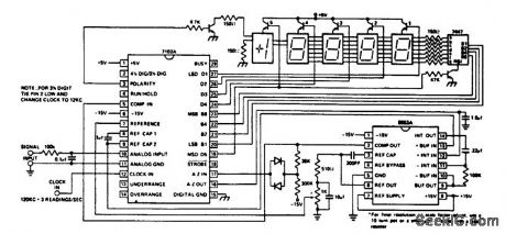
4 1/2-digit (2.000-volt) A/D converter with LED readout using the 8052A/7103A digital pair (courtesy Intersil, Inc.). (View)
View full Circuit Diagram | Comments | Reading(1069)
4_watt_audio_power_amplifier_using_an_ECG1102_as_an_AF_driver
Published:2009/7/20 5:11:00 Author:Jessie
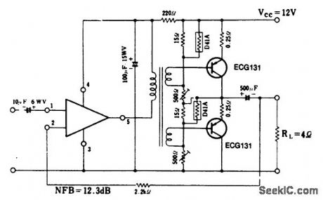
4-watt audio power amplifier using an ECG1102 as an AF driver. The ECG1102 is a 5-pin module. The two bias pots in the output stage should be adjusted to provide an idle current of 15 mA. Total current at maximum output is 450 mA. Voltage gain is 28 dB. Bandwidth is from 20 hertz to 30 kilohertz (courtesy GTE Sylvania Incorporated). (View)
View full Circuit Diagram | Comments | Reading(588)
PREFERRED_01_REGU[ATION_250_V_D_C
Published:2009/7/20 5:11:00 Author:Jessie

Provides either polarity, for applications requiring superior regulation and stability. Minimum input is 290 v d-c, and minimum Esg is 150 v d-c. Maximum output is 100 ma per series lube. C4 is minimum of 4 mfd.-NBS, Handbook Preferred Circuits Navy Aeronautical Electronic Equipment, Vol. 1, Electron Tube Circuits, 1963, PC 8, p 8-2.
(View)
View full Circuit Diagram | Comments | Reading(856)
250_mW_babysitter_intercom_using_an_LM3909_chip
Published:2009/7/20 5:10:00 Author:Jessie
250 mW babysitter intercom using an LM3909 chip. Circuitry inside dashed lines is the LM3909. Operating current is 12to 15mA (courtesy National Semiconductor Corporation). (View)
View full Circuit Diagram | Comments | Reading(597)
Parallel_gray_to_binary_converter
Published:2009/7/20 5:10:00 Author:Jessie
Parallel gray-to-binary converter(courtesy Motorola Semiconductor Products Inc.). (View)
View full Circuit Diagram | Comments | Reading(1549)
1_KW_A_C_PHASE_CONTROL
Published:2009/7/20 5:09:00 Author:Jessie

Inverse-parallel circuit is economical for manual control of lights, heaters, ovens, or fans.- Silicon Controlled Rectifier Manual, Third Edition, General Electric Co., 1964, p 138. (View)
View full Circuit Diagram | Comments | Reading(505)
8_bit_multiplying_D_A__converter_In_bipolar_operation
Published:2009/7/20 5:09:00 Author:Jessie

8-bit multiplying D/A converter In bipolar operation(courtesy Analog Devices, Inc.). (View)
View full Circuit Diagram | Comments | Reading(773)
10_KV_R_F_OSCILLATOR_TYPE_CRT_SUPPLY
Published:2009/7/20 5:09:00 Author:Jessie

Associated regulator controls oscillator output. Considered less desirable than a-f oscillator supplies, which have no r-f radiation problem.-NBS, Handbook Preferred Circuits Navy Aeronautical Electronic Equipment, Vol. 1, Electron Tube Circuits, 1963, p N14-3. (View)
View full Circuit Diagram | Comments | Reading(657)
Twelve_10_bit_CMOS_A_D_converters_onto_a_data_bus
Published:2009/7/20 5:09:00 Author:Jessie

Twelve 10-bit CMOS A/D converters onto a data bus (courtesy Analog Devices, Inc.). (View)
View full Circuit Diagram | Comments | Reading(750)
UJT_SCR_REGULATED_A_C_SUPPLY
Published:2009/7/20 5:08:00 Author:Jessie

Component values shown give optimum regulation at 25 v rms output, with less than 0.1 v variation for change in line voltage from 115 v to 100 v. For wider range of output voltage than 10 to 30 v, R1 and R4 can be ganged pot.- Transistor Manual, Seventh Edition, General Electric Co., 1964, p 334. (View)
View full Circuit Diagram | Comments | Reading(825)
| Pages:895/2234 At 20881882883884885886887888889890891892893894895896897898899900Under 20 |
Circuit Categories
power supply circuit
Amplifier Circuit
Basic Circuit
LED and Light Circuit
Sensor Circuit
Signal Processing
Electrical Equipment Circuit
Control Circuit
Remote Control Circuit
A/D-D/A Converter Circuit
Audio Circuit
Measuring and Test Circuit
Communication Circuit
Computer-Related Circuit
555 Circuit
Automotive Circuit
Repairing Circuit