
Circuit Diagram
Index 888
5_kHz_TO_2_MHz_VOLTAGE_TO_FREQUENCY_CONVERTER
Published:2009/7/9 5:28:00 Author:May

View full Circuit Diagram | Comments | Reading(613)
HEATER_VOLTAGE_REGULATOR
Published:2009/7/20 4:40:00 Author:Jessie

Clipping action is combined with depression of flat-top portion of output waveform in proportion to input voltage change, to hold rms output voltage constant within 0.2% of voltage determined by value of R5.-J. D. Wells, Low-Cost Adjustable Regulator Consumes Little Power, Electronics, 38:23, p 109-110. (View)
View full Circuit Diagram | Comments | Reading(665)
_MODEL_TRAIN_THROTTLE_CONTROL
Published:2009/7/9 5:27:00 Author:May


What makes this control unique is its momentum feature, which adds a degree of realism. The circuit will operate well for trains that draw up to 1 A at 15 V. None of the components are critical.In the start mode, current source Q1 charges capacitor C1. The charge current and start-up time are adjusted by resistor R2. In the stop mode, current-sink Q2 discharges capacitor C1. The discharge current and stop time are set byresistor R4. In the coast mode, op amp U1 draws very little current from C1, so the speed will remain nearly constant for some time, and then gradually decrease. Transistors Q3 and Q4 form a Darlington emitter-follower to amplify the output of U1. Diode D7 reduces the output by about 0.8 V. Another diode could be added in series to decrease the output to 0 in the stop mode. (View)
View full Circuit Diagram | Comments | Reading(1650)
F_V_converter_having_0_to__5_volt_output_with_a_5_kHz_to_10_kHz_input
Published:2009/7/20 4:40:00 Author:Jessie

F/V converter having 0 to +5-volt output with a 5 kHz to 10 kHz input (courtesy Analog Devices, Inc.). (View)
View full Circuit Diagram | Comments | Reading(864)
VOLTAGE_REGULATOR_FOR_CARS_AND_MOTORCYCLES
Published:2009/7/9 5:26:00 Author:May
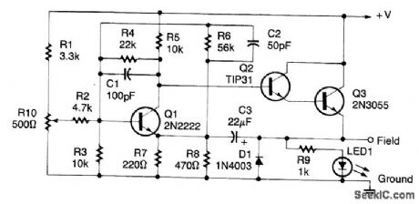
This regulator circuit can be used on an alternator that has one field terminal grounded. When +V (input) gets too high, Q1 conducts, and the base of Q2 is driven toward ground, reducing the voltage fed to Q3. This lowers the voltage fed to the field of the altemator. (View)
View full Circuit Diagram | Comments | Reading(3077)
10_bit_buffered_multiplying_D_A_convener_for_two_quadrant_multiplication
Published:2009/7/20 4:39:00 Author:Jessie

10-bit buffered multiplying D/A convener for two-quadrant multiplication (courtesy Analog Devices, Inc.). (View)
View full Circuit Diagram | Comments | Reading(971)
BALANCE_INDICATOR
Published:2009/7/9 5:26:00 Author:May

If your amplifier is fitted with two level controls, it actually offers you a balance control and a level control. A drawback of this is that it is quite difficult to set the balance properly. This can be obviated, however, by replacing the two monopotentiometers with stereo versions P1 and P2 in the diagram.
One half of the pair, P1A and P2A, assumes the tasks of the removed components. The other half is connected in a bridge circuit. The voltage between wipers of the potentiometers is then a measure of the balance between the two channels. The lower the potential, the better the balance. If you are interested in knowing the degree of unbalance, connect a center-zero moving coil meter with a bias resistor between A and B. With this arrangenient, zener diodes Dl and D2 can be omitted: they are necessary only with the LED indicator shown in the diagram to prevent the input voltage of the op amp from getting too close to the level of the supply voltage.
The circuit around IC1 is a classical differential amplifier. Resistors R5 and R6 provide a virtual earth for the LEDs, which is necessary to ensure that, in spite of the asymmetrical supply voltage, a positive and a negative output is obtained.
Because the LEDs have been included in the feedback loop of the indicator, the circuit is pretty sensi-tive. At only 40 mV, that is, just 1/400 of the supply voltage, one of the LEDs begins to light. The maximum current drawn by the LEDs is determined by the values of R5 and R6. (View)
View full Circuit Diagram | Comments | Reading(737)
35_watt_OTL_audio_power_amplifier_using_an_ECG1029
Published:2009/7/20 4:39:00 Author:Jessie

3.5-watt OTL audio power amplifier using an ECG1029. Voltage gain at 1 kHz is 44 dB (courtesy GTE Sylvania Incorporated). (View)
View full Circuit Diagram | Comments | Reading(567)
WINDSHIELD_WIPER_INTERVAL_CONTROLLER
Published:2009/7/9 5:25:00 Author:May

The windshield wiper interval circuit presented here is very compact and is noteworthy for its use of two thyristors, instead of a relay. It has only two connections and operates without any problemseven in conjunction with multistage wiper circuits.
The connecting wire between the wiper motor and terminal S3 is cut and new connections are made (as shown in the diagram). When the interval switch, S1, is closed, capacitor C1 charges via P1 and the wiper motor. After a time set with P1, transistor T1 switches on and triggers the thyristors. The wiper motor is then energized via the thyristors and D3 and sets the wipers into motion. At the same time, C1 discharges via D2 and the thyristors.
After a short time, the wiper stop switch con-nects terminal 53 to the +12-V line so that the wiper motor is energized via D4. The thyristors are switched off because the voltage drop across D3 plus Th1/Th2 is then greater than that across D4. When the wipers reach the end of their travel again, the stop switch connects terminal 53 to ground and enables C1 to charge again. (View)
View full Circuit Diagram | Comments | Reading(1187)
100_V_D_C_REGULATOR
Published:2009/7/20 4:39:00 Author:Jessie

Provides up to 400 ma at 100 v with 1% regulation for inputs of 101 to 150 v from unregulated source. Auxiliary source Ea must be minimum of 5 v.-NBS, Handbook Preferred Circuits Navy Aeronautical Electronic Equipment, Vol. 11, Semiconductor Device Circuits, PSC 5, p 5-2.
(View)
View full Circuit Diagram | Comments | Reading(636)
DIFFERENTIAL_PREAMP
Published:2009/7/9 5:23:00 Author:May

Opamps A1 and A2 form cross-coupled preamp with differential input and differential output, driving instrumentation opamp A3 to provide overall gain of 106. Common-mode input range is ±10 V, and full.scale differential input is ±100 mV. For higher input impedance, 108 opamps can be used in preamp. For higher speed, all three opamps can be 118.-W. G. Jung, IC 0p-Amp Cookbook, Howard W. Sams, Indianapolis, IN, 1974, p 241-243. (View)
View full Circuit Diagram | Comments | Reading(1394)
10_bit_buffered_multiplying_D_A_converter_in_bipolar_operation_
Published:2009/7/20 4:38:00 Author:Jessie

10-bit buffered multiplying D/A converter in bipolar operation (courtesy Analog Devices, Inc.). (View)
View full Circuit Diagram | Comments | Reading(732)
ad_dc_INDICATOR
Published:2009/7/9 5:22:00 Author:May

By using two switching transistors and two LEDs, this circuit can distinguish low-level ac and dc sig-nals. If the red LED illuminates, the signal is positive dc. If the yellow LED lights, the signal is negative dc.If the signal is ac, both LEDs will light. (View)
View full Circuit Diagram | Comments | Reading(665)
F_V_convener_used_for_FM_demodulation
Published:2009/7/20 4:38:00 Author:Jessie

F/V convener used for FM demodulation. The example shown here has the carrier at 50 kHz with ±5 kHz modulating signal. The terms shown are defined as follows: G is gain, RF is the external gain resistor, △Es is the output offset shift and Rc is the offset current resistor (courtesy Analog Devices, Inc.). (View)
View full Circuit Diagram | Comments | Reading(804)
MODEL_TRAIN_AND_SLOT_CAR_CONTROLLER
Published:2009/7/9 5:21:00 Author:May

As shown, a 555 timer (U1) is configured as an astable multivibrator (oscillator) with a 400:1 duty cycle and a frequency of 40 Hz.When power is applied to the circuit, capacitor C1 (connected to pin 6 of U1) is discharged and the output of the 555 (which is used to sink current) is low. Capacitor C1 begins to charge via RI and R2 toward the positive supply rail. When the charge on C1 reaches about 66% of +V, the output of U1 at pin 3 goes high.At that point, C1 begins to discharge through R2. When the charge on C1 decreases to about 33% of the supply voltage, the output of U1 returns to the low state, and the cycle is repeated until power is removed from the circuit.When the output of U1 is low, C3 is discharged into U1 via transistor Q2. When U1 pin 3 goes high, C3 charges thr2ough a current source that consists of D1, D2, R3, R4, and Q1. The charge/discharge cycling of C3 produces a stream of pulses that are fed to the inverting inputs of U2A and U2B (an LM358 dual op amp). Two voltage-di ider networks (R7, R8, R9, and R10, R11, R12) set the reference voltage that is applied to the noninverting inputs of U1A and U1B at pins 3 and 5.Potentiometers R9 and R12 set the low-level duty cycle (5 to 10%) of U1A and U1B. They are adjusted so that the train head-lights glow, but the motor hums only slightly. Potentiometer R3 adjusts the ramp rate of C3 for 100% duty cycle at the full throttle setting. A double-pole, single-throw switch (S1A and S1B) is used to place R3/C4 and R4/C5 in the circuit.The R5/C4 and R6/C5 combinations cause the reference voltages presented to the noninverting inputs to U2A and U2B to change very slowly when the throttle is turned up and down. When the ACL/DCL switch is turned off, the resistance of the throttle-divider networks are much smaller than those of R5 and R6, so the reference voltages on C4/C5 change instantly to the new throttle setting.The output drivers consist of resistors R13 and R15, and transistors Q3 and Q4 for output A'; and resistors R17 to R20, and transistors Q5 and Q6 for output B. Components R13/R16/Q3 and R17/R20/Q5 limit the output drive currents of Q4 and Q6 to about 3 A each. Resistors R14/R15 and R18/R19 turn on Q4 and Q5, respectively, before the breakover voltage is reached to prevent damage to the output drivers and dissipate the energy that is stored in an inductive field (such as in a motor).The power supply delivers 18 V to the track. Voltage regulator U3 (a 78L09 9-V, 100-mA voltage regulator) supplies power to the control circuits.
(View)
View full Circuit Diagram | Comments | Reading(1492)
WIDE_RANGE_VOLTAGE_TO_FREQUENCY_CONVERTER_1
Published:2009/7/9 5:21:00 Author:May
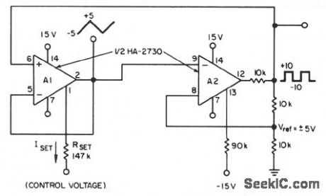
This circuit uses a programmable op amp such as the HA2730-a two-amplifier monolithic chip with independent programming ports for each amplifter-whose slew rate and other parameters vary linearly with a so-called set current. The converter circuit uses one amplifier, A1, as a slewing amplifier and other, A2, as a comparator function. The control voltage VC, determines A1's slew rate. And, because A1's output voltage swing is constant, the modulation of its set current results in direct control of the circuit's frequency. A1's internal compensation capacitor acts as the timing component. An internal bipolar current source,whose current magnitude is directly proportional to the set current of pin 1, then determines the charge-discharge rate. A conversion nonlinearity of ±0.03% of full scale over 3 decades and ±1.5% of full scale over4.3 decades of frequency is possible. The frequency range is adjustable by a change in the resistance R. (View)
View full Circuit Diagram | Comments | Reading(616)
HIGH_POWER_CAR_AUDIO_AMPLIFIER
Published:2009/7/9 5:21:00 Author:May
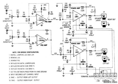
This stereo amp will supply 60 W rms into 8Ω or 100 W rms into 4Ω. Notice that the LM12C1 line level (about 300 mV) into 5 KΩ. A±35-V supply is required for full power output. Power can be obtained from a dc-dc converter. (View)
View full Circuit Diagram | Comments | Reading(1254)
A_C_LINE_REGULATOR
Published:2009/7/20 4:26:00 Author:Jessie

Five-transistor circuit uses breakdown diodes to regulate voltage inputs between 113 v and 140 v to within 0.5 v of 110 v for 2-amp load.-R. A. Grainer, Line Voltage Control Uses Zener Diodes, Electronics, 33:6, p 64. (View)
View full Circuit Diagram | Comments | Reading(582)
as_CIRCUIT_LED_POWER_INDICATOR
Published:2009/7/9 5:21:00 Author:May

Many electronic circuits need an indication that they are under power; for most ac circuits, a neon lamp is the device of choice. A bidirectional tricolor LED can be used if a capacitor is connected in series with the LED to limit the current through the LED. A1-μF, 250-WVdc capacitor, which has a reactance of 2650 ohms at 60 Hz, is used in series with an LED to limit the current through the unit to 43 mA. The impedance of the LED is low compared to the reactance of the capacitor, so nearly al the impedance will be caused by the capacitor with the added advantage of no energy loss caused by the capacitor.
The power of the LED is 1.175Vx0.043 A=50 mW compared to an NE-2H at 250 mW. For 230V, use a 0.47-μF, 400-WVdc capacitor. (View)
View full Circuit Diagram | Comments | Reading(892)
15_watt_AF_power_amplifier_using_an_ECG1059_chip_and_two_ECG175_bipolar_transistors
Published:2009/7/20 4:38:00 Author:Jessie

15-watt AF power amplifier using an ECG1059 chip and two ECG175 bipolar transistors. Minimum voltage gain is 63 dB. Maximum input voltage is 1 mV for the given output (courtesy GTE Sylvania Incorporated). (View)
View full Circuit Diagram | Comments | Reading(586)
| Pages:888/2234 At 20881882883884885886887888889890891892893894895896897898899900Under 20 |
Circuit Categories
power supply circuit
Amplifier Circuit
Basic Circuit
LED and Light Circuit
Sensor Circuit
Signal Processing
Electrical Equipment Circuit
Control Circuit
Remote Control Circuit
A/D-D/A Converter Circuit
Audio Circuit
Measuring and Test Circuit
Communication Circuit
Computer-Related Circuit
555 Circuit
Automotive Circuit
Repairing Circuit