
Circuit Diagram
Index 896
10_bit_CMOS_A_D_converter_in_unipolar_binary_operation_
Published:2009/7/20 5:08:00 Author:Jessie


10-bit CMOS A/D converter in unipolar binary operation (courtesy Analog Devices, Inc.). (View)
View full Circuit Diagram | Comments | Reading(851)
REAR_FOG_LIGHT_CONTROLLER_WITH_DELAY
Published:2009/7/9 4:51:00 Author:May

We assume that most of our readers are thoughtful drivers who do not switch on their rear fog lights when closely followed by other traffic. Following drivers (for an instant) will think that you are braking (although they have seen no reason for your doing so) and thus slam on their brakes as well. This could cause a very dangerous situation. Avoid a potentially dangerous action and install the rear fog light delay circuit, presented here.
Switch S1 is the on/off control for rear fog lights L1 and L2. As soon as this switch is closed, the gatesource voltage (Vgs) of MOSFET T1 will become more and more negative. Thus, the IC will conduct harder and harder. This in turn causes the brightness of the lights to gradually become brighter. Maximum brightness is reached after a delay of about 20 seconds, which is determined by time constant R2/C1.
The gate of T1 can be given a bias by preset Pl. This provides compensation for the initial period after the lights are switched on and the lamps do not light, because they need hundreds of milliamperes before they can do so. With Pl set correctly, the lamps will light, albeit weakly, and immediately the control switch is closed. The gate potential is then equal to the voltage at the wiper of Pl (remember that C1 is then still discharged).
Although the dissipation of T1 is a maximum during the transitional period (between switch on and the lamps lighting brightly), the heatsink required is calculated on the basis of the dissipation when the lamps light brightly. (View)
View full Circuit Diagram | Comments | Reading(789)
ELECTRONIC_DICE
Published:2009/7/9 4:51:00 Author:May

When S1 is pressed, counter U2 is driven by oscillator U1A/U1B and the count (0 through 6) is read on DISP1. R1 and C1 determine the count rate, which should be fast enough to ensure a random count. (View)
View full Circuit Diagram | Comments | Reading(0)
15_watt_20_watt_AF_amplifier_using_complementary_Darlington_output_transistors
Published:2009/7/20 5:08:00 Author:Jessie

15-watt/20-watt AF amplifier using complementary Darlington output transistors. To ensure maximum signal swing the junction of R8 and R9 should be half-Voc (courtesy Motorola Semiconductor Products Inc.). (View)
View full Circuit Diagram | Comments | Reading(1794)
12_TO_16_V_CONVERTER
Published:2009/7/9 4:49:00 Author:May
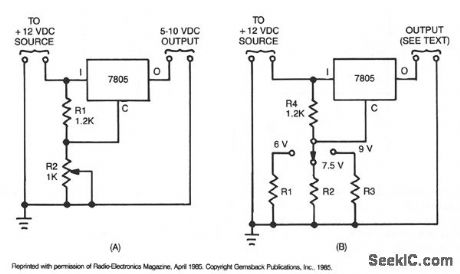

Many devices operate from a car's 12-V electrical system. Some require 12 V; others requtre some lesser voltage. An automobile battery's output can vary from 12 to 13.8 V under normal circumstances. The load requirements of the device might vary. This circuit maintains a constant voltage regardless of how those factors change. Simple circuit, A, uses a 7805 voltage regulator. In addition to a constant output, this IC provides overload and short-circuit protection. That unit is a 5-V, 1-A regulator, but when placed in circuit B, it can provide other voltages as well. When the arm of potentiometer R1 is moved toward ground, the output varies from 5 to about 10 V. (View)
View full Circuit Diagram | Comments | Reading(652)
CAR_LIGHTS_MONITOR
Published:2009/7/9 4:48:00 Author:May


This circuit is for the purpose of monitoring automotive lighting. Two special ICs are available from Telefunken that are designed to measure the current through a light bulb. In practice, detecting whether a current flows through a bulb or not is a most suitable way of determining whether the bulb still works.
If a small resistance is connected in series with a bulb, a small voltage drop will develop across it when the bulb lights (R1 and R2 in the diagram). Each IC can cope with only two bulbs, so three or four ICs are needed per car. The junction of the bulb and resistor is connected to one of the inputs (pin 4 or pin 6) of the IC. The potential across the resistor is compared in the IC with an internal reference voltage. Depend-ing on which of the tWo ICs is used, the voltage drop must be about 16 mV (U477B) or 100 mV (U478B). This voltage drop is so small that it will not affect the brightness of the relevant bulb.
The value of the series resistor is determined quite easily. If, for instance, it is in series with the brake light (normally 21 W), the current through the bulb, assuming that the vehicle has a 12-V battery, is 21÷12=1.75 A. The resistance must then be of 16÷1.75=9 mΩ (U477B) or 100÷1.75=57 mΩ (U478B).
These resistors can be made from a length of resistance wire (available from most electrical retailers).Failing that, standard circuit wire of 0.7 mm diameter can be used. This has a specific resistance of about 100 mΩ per meter. However, in most cars, the existing wiring will have sufficient resistance to serve as series resistor.
LEDs can be connected to the outputs of the IC (pins 3 and 5). These will only light if the relevant car light fails to work properly. (View)
View full Circuit Diagram | Comments | Reading(1201)
SIMPLE_LIE_DETECTOR
Published:2009/7/9 4:48:00 Author:May

The variation in skin resistance of the subject is used to vary contact rings are two brass rings, about 3/4 ID. (View)
View full Circuit Diagram | Comments | Reading(0)
IF_POSITIVE_VSUBREF_SUB_IS_USED
Published:2009/7/20 5:06:00 Author:Jessie

IF POSITIVE VREF IS USED.THE ANALOG INPUT RANGE IA 0 TO-VREF,AND THE COMPARTOR'S㈠ INPUT SHOULD BE CONNECTED TO OUT1(PIN 4) OF THE AD7570. (View)
View full Circuit Diagram | Comments | Reading(829)
4_INPUT_UNITY_GAIN_MIXER
Published:2009/7/9 4:45:00 Author:May
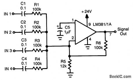
An LM381/1Ais used as a four-input unity-gain audio mlxer. Gain can be increased decreasing R1 through R4 or increasing R6. (View)
View full Circuit Diagram | Comments | Reading(2854)
DUAL_OUTPUT±12_OR±15_V_DC_DC_CONVERTER
Published:2009/7/9 4:44:00 Author:May

The buck-boost configuration of the MAX634 is well suited for dual output dc-dc converters Only a second winding on the inductor is needed. Typically, this second winding is bifilar-primary and secondary are wound simultaneously using two wires in parallel. The inductor core is usually a toroid or a pot core. The negative output voltage is fully regulated by the MAX634. The positive voltage is semiregulated, and will vary slightly with load changes on either the positive or negative outputs. (View)
View full Circuit Diagram | Comments | Reading(1239)
REMOTELY_ADJUSTABLE_SOLID_STATE_HIGH_VOLTAGE_SUPPLY
Published:2009/7/9 4:43:00 Author:May
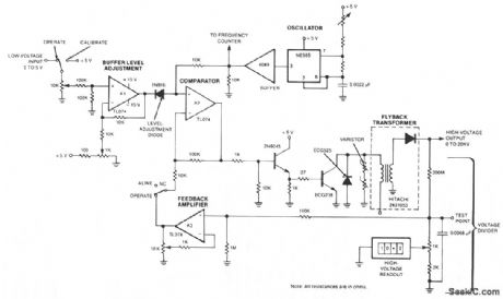
The output voltage changes approximately linearly up to 20 KV as the input voltage is varied from 0 to 5 V. The oscillator is tuned by a 5-Ω potentiometer to peak the output voltage at the frequency of maximum transformer response between 45 and 55 kHz. The feedback voltage is applied through a 100-KΩ resistor, an op amp, and a comparator to a high-voltage amplifier. A diode and varistors on the primary side of the transformer protect the output transistor. The transformer is a flyback-type used in color-television sets. A feedback loop balances between the high-voltage output and the low-voltage input. (View)
View full Circuit Diagram | Comments | Reading(754)
WHEEL_OF_FORTUNE
Published:2009/7/9 4:41:00 Author:May

This circuit is a 10-LED spinning wheel that clicks as the wheel passes each point. The rotation starts fast, then gradually slows down to a random stop (with a click at each position). After the rotation ceases, the selected LED stays lit for about 10 seconds, then goes out. The cycle restarts by depressing (View)
View full Circuit Diagram | Comments | Reading(3010)
15_W_OFFLINE_CONVERTER
Published:2009/7/9 4:41:00 Author:May

This nonisolated, unregulated, minimum component converter fills the void between low-power zener regulation and the higher power use of a 60-Hz input transformer. It is intended for use wherever a nonisolated supply can be used safely.The circuit operates by conducting only during the low-voltage portion of the rectified sine wave. R1 and D2 charge C1 to approximately 20 V, which is maintained by Q1. This voltage is applied to the gate of Q2, turning it on. When the rectified output voltage exceeds the zener voltage of D4, Q1 turns on, shunting the gate of Q2 to ground, turning it off. (View)
View full Circuit Diagram | Comments | Reading(621)
DIGITAL_MIXER
Published:2009/7/9 4:40:00 Author:May

A simple digital mixer, based on two dual-Schmitt triggers (4583B) and three exclusive-OR gates, uses an RC time-delay circuit to permit easy adjustment of the output-signal pulse width. The exclusive-OR gates ,can also be used separately as a symmetrical frequency doublet.As shown, a signal passing through the Schmitt triggers is delayed by t, a value equal to RC In (VTP/VTN)where Vtp and Vtn are the positive and negative threshold voltages of the triggers.To function properly, the same time delay must be introduced to signals f1 and f2. Also, the time delay must be less than 50%of the period of f1. Provided that f1 is more than twice the value of f2, the output of the circuit will equal the difference of the two signals (i.e., f1 - f2). (View)
View full Circuit Diagram | Comments | Reading(2320)
BACK_UP_ALARM
Published:2009/7/9 4:40:00 Author:May

The brake lights of the automobile trigger this circuit on and off. This saves the annoyance of the alarm when it is not needed. (View)
View full Circuit Diagram | Comments | Reading(1026)
LOW_CURRENT_SIMPLE_CMOS_ALARM
Published:2009/7/9 4:39:00 Author:May

This CMOS-aided alarm draws only 1μA standby current. An open sensor allows IC1 to bias Q1 on, activating RY1. (View)
View full Circuit Diagram | Comments | Reading(557)
RUN_DOWN_CLOCK_SOUND_GENERATOR
Published:2009/7/9 4:39:00 Author:May

Used in electronic roulette or dice games, this circuit produces a clock signal that initially is several tens of kHz (depending on C2) and gradually decreases to zero in about 15 seconds, as C1 discharges through R4. (View)
View full Circuit Diagram | Comments | Reading(911)
REGULATED_15_VSUBOUT_SUB_6_V_DRIVEN_CONVERTER
Published:2009/7/9 4:37:00 Author:May
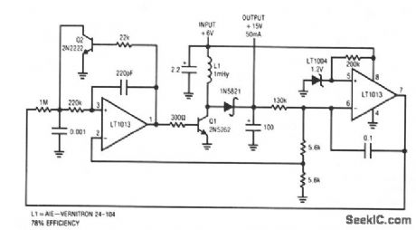
This converter delivers up to 50 mA from a 6-V battery with 78% efficiency. This flyback converter functions by feedback-controlling the frequency of inductive flyback events. The inductor's output, rectifted and filtered to dc, biases the feedback loop to establish a stable output. If the converter's output is below the loop setpoint, A2's inputs unbalance and current is fed through the 1-MΩ resistor at A1. This ramps the 1000-pF value positive. When this ramp exceeds the 0.5-V potential at A1's positive input, the amplifier switches high. Q2 turns on, discharging the capacitor to ground. Simultaneously, regenerative feedback through the 200-pF value causes a positive-going pulse at A1's positive input, sustaining Al's positive output. Q1 comes on, allowing inductor, L1, current to flow. When Al's feedback pulse decays, its output becomes low, turning off Q1. Q1's collector is pulled high by the inductor's flyback and the energy is stored in the 100-μF capacitor. The capacitor's voltage, which is the circuit output, is sampled by A2 to close a loop around A1/Q1. This loop forces A1 to oscillate at whatever frequency is required to maintain the 15-V output.In-phase transformer windings for the drain and gate of TMOS power FET Q1 cause the circuit to oscillate. Oscillation starts when the feedback coupling capacitor, C1, is charged from the supply line via a large resistance; R2 and R3 limit the collector current to Q2. During pump-up the on time is terminated by Q2, which senses the ramped source current of Q1. C1 is charged on alternate half-cycles by Q2 and forward-biased by zener D2.When the regulated level is reached, forward bias is applied to Q2, terminating the on time earlier at a lower peak current. When this occurs, the frequency increases in inverse proportion to current, but the energy per cycle decreases in proportion to current squared. Therefore, the total power coupled through the transformer to the secondary is decreased. (View)
View full Circuit Diagram | Comments | Reading(512)
FET_BIPOLAR_DARLINGTON
Published:2009/7/9 4:37:00 Author:May

Can be used as meter interface amplifier, impedance transformer, coax driver, or relay actuator. Combination of unipolar and bipolar transistors gives desirable amplifying features of each solid-state device.-I. M. Gottlieb, A New Look at Solid-State Amplifiers, Ham Radio, Feb. 1976, p 16-19. (View)
View full Circuit Diagram | Comments | Reading(1710)
SINGLE_IC_ALARM
Published:2009/7/9 4:36:00 Author:May

With a single IC, you can build a simple, reliable auto burglar alarm or a similar alarm. See (a) for the timing information for the alarm circuit in (b).
When you leave your vehicle, flip the arming switch and close the door,behind you to arm the device.Subsequent opening of an entrance triggers both timers. After the expiration of the entry delay timer, the alarm sounds for a time that is determined by the second timer.
The value of R should be less than 1 kΩ. If you use an incandescent lamp instead of a resistor, you get an extra function-an open-entrance indicator. By keeping the resistance low, you avoid false tripping should water collect under the hood.
If your door switch connects the courtesy light to 12 V rather than to ground, use a single transistor as an inverter at the input. Although this circuit's simplicity has its drawbacks, you can add more features, such as no-entry delays for the hood and trunk, and retripping when doors remain open. (View)
View full Circuit Diagram | Comments | Reading(701)
| Pages:896/2234 At 20881882883884885886887888889890891892893894895896897898899900Under 20 |
Circuit Categories
power supply circuit
Amplifier Circuit
Basic Circuit
LED and Light Circuit
Sensor Circuit
Signal Processing
Electrical Equipment Circuit
Control Circuit
Remote Control Circuit
A/D-D/A Converter Circuit
Audio Circuit
Measuring and Test Circuit
Communication Circuit
Computer-Related Circuit
555 Circuit
Automotive Circuit
Repairing Circuit