
Circuit Diagram
Index 889
ELECTRONIC_IGNITION
Published:2009/7/9 5:18:00 Author:May

This electronic ignition circuit is intended to be inserted into a car's conventional ignition system. In effect, it replaces the original 12-V switching circuit in the primary winding of the coil by one generating more than 100 V. It thereby converts a current circuit, which is upset by lead and stray resistance, into a voltage circuit that is much more efficient.
The pulses emanating from the contact breaker, shown at the extreme lower left-hand side of the dia-sram, are applied to transistor T1 and subsequently differentiated by R3/C1. This causes a negligible igni-tion delay. The current through the contact-breaker points is determined by the value of R1. This value has been chosen to ensure that the points remain clean.
Transistor T1 is followed by two monostables, IC1A and IC1B, which are both triggered by the output pulses of T1. However, whereas IC1A is triggered by the trailing edge, IC1B is triggered by the leading edge.
Monostable IC1A passes a pulse of about 1.5 ms (determined by R4/C2) to NAND gate IC2A. This gate switches off high-voltage Darlington T3 via gates IC2B, IC2C and IC2D, and driver T2, for the dura-tion of the pulse. Gate IC2 ensures that T3 is switched on only when the engine is running, to prevent a current of some amperes flowing through the ignition coil.
As long as pulses emanate from the contact breaker, ICIB is triggered and its Q output remains logic high. The mono time of this stage is about 1 s and is determined by R5/C3.
Darlington T3 is switched on via T2 and IC2A through IC2D as long as IC1A does not pass an ignition pulse. When the engine is not running, the Q output of IC2B goes low after 1 s and this causes T2 and T3 to be switched off. The two series-connected 180-V zener diodes protect the collector of the BU932R against too high of a voltage. The Darlington must be fitted on a suitable heatsink. (View)
View full Circuit Diagram | Comments | Reading(6440)
A_D_converter_with_sample_and_hold_circuit_for_unipolar_operation_0_to_10_volts
Published:2009/7/20 4:37:00 Author:Jessie

A/D converter with sample-and-hold circuit for unipolar operation, 0 to 10 volts. For operation of 0 to 5 volts jumper pins 22 and 25 with the connection shown (courtesy Datel Systems, Inc.). (View)
View full Circuit Diagram | Comments | Reading(973)
VISUAL_CW_OFFSET_INDICATOR
Published:2009/7/9 5:17:00 Author:May

An NE567 tone decoder, tuned to the transceiver's CW offset frequency, ensures that the transceiver will be transmitting on the same frequency as the received CW signal. Simply tune the transceiver so that the LED lights. Eight to 13 Vdc is required; this can be taken from the transceiver supply or an extra battery. Audio is taken from the speaker or headphone output. (View)
View full Circuit Diagram | Comments | Reading(1027)
High_gain_AF_preamplifier_using_an_ECG1053_chip
Published:2009/7/20 4:37:00 Author:Jessie
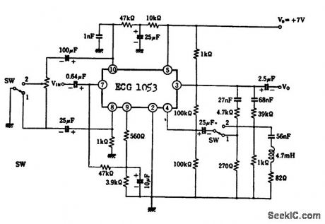
High-gain AF preamplifier using an ECG1053 chip. Frequency response is from 30 hertz to 15 kilohertz. Minimum voltage gain is 93 dB (courtesy GTE Sylvania Incorporated). (View)
View full Circuit Diagram | Comments | Reading(725)
HIGH_CMRR
Published:2009/7/9 5:15:00 Author:May
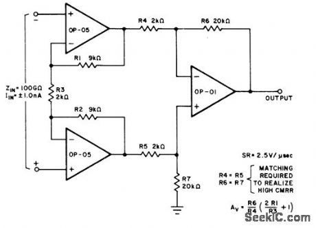
Use of two Precision MonolithIcs OP-05 opamps feeding OP-01 opamp gives input impedance of about 100 gigohms and high common-mode rejection for instrumentationapplications. -'' lnstrumentation Operational Amplifier, Precision Monolithics, Santa Clara, CA, 1977, OP-05, p 7. (View)
View full Circuit Diagram | Comments | Reading(923)
F_V_converter_with___10000_volt_full_scale_output_and_fine_trim_adjustment
Published:2009/7/20 4:36:00 Author:Jessie

F/V converter with + 10.000 volt full scale output and fine trim adjustment (courtesy Analog Devices, Inc.). (View)
View full Circuit Diagram | Comments | Reading(929)
TRANSISTORIZED_BAR_GRAPH_DRIVER
Published:2009/7/9 5:15:00 Author:May

A resistor network (R1 through R10) with emitter followers (Q1 and Q2) drives LED drivers (Q3 through Q7). This circuit was used as a light organ to provide visual volume indication. It can be hooked to a speaker, to another audio source, etc. (View)
View full Circuit Diagram | Comments | Reading(846)
SOLID_STATE_WINDSHIELD_WIPER_DELAY
Published:2009/7/9 5:13:00 Author:May
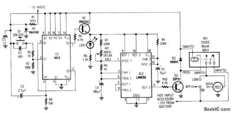
In the wiper-delay schematic shown, with the ignition on, D1 maintains regulated + 12 Vdc. When S1 closes, C1 bypasses transients and passes this + 12 Vdc to divider R2-R3, producing a TTL high at pin 3 of IC1, a 4013 CMOS dual leading-edge triggered D-type flip-flop. Filter R4/C3 keeps IC1 from triggering erroneously when the ignition is on. When S1 is pressed, output Q1 (pin 1) of IC1 latches high, turning on Q1, which conducts via R5, turning on IC2; LED1 indicates power, and R6 sets the current. Because IC2 depends on Q1 for power, IC2 stays off until Q1 turns on.
The left half of IC2 is an astable, with its delay set by R7, R8, R11, and C4. The right half of IC2 is a monostable, with its pulse duration set by R9 and C5. With the values used, you might expect R11 to vary the delay from about 15 to 84 seconds, with a 2.42-second monostable pulse operating the wiper blades on each cycle. However, the actual delay will range between 2 to 18 s, with a 1-s monostable pulse on each cycle. That discrepancy stems from the fact that IC2 is being fed from the emitter of Q1, rather than directly from the regulated +12-V supply. Transistor Q1 acts as an active current source, charges and discharges C4 faster than it ordinarily would.
The astable output (OUT1, pin 5) is tied to TRIG2 (pin 8). When OUT2 (pin 9) becomes high, Q2 is biased via RIO and current flows through RY1, with D2 dissipating back-emf when RY1 shuts off. (View)
View full Circuit Diagram | Comments | Reading(2419)
D_C_SWITCHED_REGULATOR
Published:2009/7/20 4:36:00 Author:Jessie

Gives 0.5% regulation for input voltage range from -15% to +30%. Efficiency is 95%. Transistor is near-ideal switch, having low leakage when open and low voltage when closed.-A. A. Sorenson, Solid-State D-C Switched Regulators, Electronics, 33:48, p 121-123. (View)
View full Circuit Diagram | Comments | Reading(684)
F_V_convener_with__10_volt_full_scale_output_and_decreased_threshold_for_increased_triggering_sensitivity_for_low_level_input_signals
Published:2009/7/20 4:36:00 Author:Jessie

F/V convener with +10-volt full scale output and decreased threshold for increased triggering sensitivity for low-level input signals. The input frequency range is 0 to 11 kHz for the 451 and 110 kHz for the 453 (courtesy Analog Devices, Inc.). (View)
View full Circuit Diagram | Comments | Reading(954)
WIDE_RANGE_VOLTAGE_TO_FREQUENCY_CONVERTER
Published:2009/7/9 5:13:00 Author:May
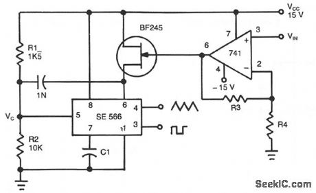
This circuit is based upon the change of frequency of the function generator with the input voltage VIN Generally, the frequency depends upon the capacitance and resistor connected to pin 6. This resistor is replaced by the FET. The frequency range is adjustable by changing the input voltage, VIN; the converter will give a range of 10 Hz to 1 MHz. (View)
View full Circuit Diagram | Comments | Reading(816)
2_watt_AF_power_amplifier_for_a_16_ohm_load_using_a_GEIC_1
Published:2009/7/20 4:35:00 Author:Jessie
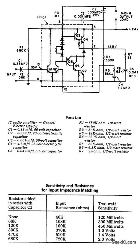
2-watt AF power amplifier for a 16-ohm load using a GEIC-1. See table for sensitivity (courtesy General Electric Company). (View)
View full Circuit Diagram | Comments | Reading(548)
AUDIO_AMPLIFIER_VOLUME_INDICATOR
Published:2009/7/9 5:12:00 Author:May

The indicator IS intended for use with an audio gmplifier or preamp⒒fter, but it can also be used in other applcations where a number of steps or changes must be counted rapidly.To prevent interferencewith the audio signal,the circuit is a static design.Thus,if the volume control is not adjusted,the circuit does nothint.
The circuit does not need an external clock signal,because this IS derived from any changes h theleast significant bit (LSB).This is done by two differentiating networks:R9/C1 and RIO/C2,which double the frequencY of an available LSB signal.
Moreover,to ensure that the counters of the indicator remain in step with the volume control,signals“up/down”and preset from the preamplifier are used.It might seem rather extravagant to couple the state of the counters in the prearnplifter with that the present counters,but it is a good way to keep the connections between the two units to a minimum,Furthermore,the present counters operate In 8-bit BCD,instead of 6-bit binary as used by those h the volume control (in the preamplifier).All that is required to display the state of the volume control are a couple of BCD-to-7-segment decoders and 7-segment displays.
The preset h the indicator must be set h BCD code,Leading zeros are not suppressed so numbers up to and including 9 are displayed,startingwith a 0,The DIP switches and resistors RI through R8 In the diagram can be omitted if only one fixed preset is likely to be used.The resistors should be replaced by jump leads. (View)
View full Circuit Diagram | Comments | Reading(2914)
F_V_converter_with__10_volt_full_scale_output
Published:2009/7/20 4:35:00 Author:Jessie

F/V converter with +10-volt full scale output. Table shows input specs for both models (courtesy Analog Devices, Inc.). (View)
View full Circuit Diagram | Comments | Reading(894)
SENSOR_BRIDGE
Published:2009/7/9 5:11:00 Author:May
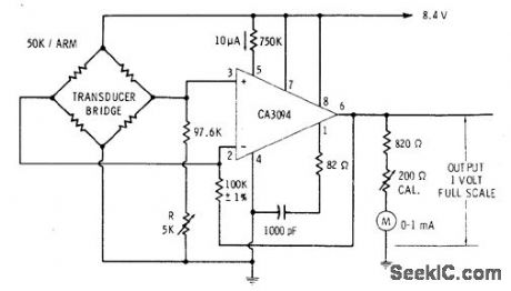
RCA CA3094 combination power switch and amplifier can be used with variety of transducer bridges for instrumentation and other applications. Circuit delivers output of 1 V full-scale for driving meter. Pot R serves as centering or reference control. Can be used as thermometer if one leg of bridge is thermistor and meter scale is calibrated in degrees. -E. M. Noll, Linear IC Principles, Experiments, and Projects, Howard W.Sams, Indianapolis, IN, 1974, p 311-313. (View)
View full Circuit Diagram | Comments | Reading(803)
LOW_COST_VOLTAGE_TO_FREQUENCY_CONVERTER
Published:2009/7/9 5:10:00 Author:May

The 741 op amp integrator signal is fed into the Schmitt trigger input of an inverter. When the signal reaches the magnitude of the positive-going threshold voltage, the output of the inverter is switched to zero. The inverter output controls the FET switch directly. For a gate voltage of zero, the FET chan-nel turns on to low resistance and the capacitor is discharged. The discharge current depends on the on resistance of the FET. When the capacitor C1 is discharged to the negative-going threshold voltage level of the inverter, the inverter output is switched to ±12 V. This switch causes the FET channel to be switched off, and the discharging process is switched into a charging process again. Using the components shown, an output frequency of about 10kHZ with 0.1% linearity can be obtained. (View)
View full Circuit Diagram | Comments | Reading(1682)
ADJUSTABLE_10_A_REGULATOR
Published:2009/7/9 5:09:00 Author:May

View full Circuit Diagram | Comments | Reading(642)
TRACKING_PREREGULATOR
Published:2009/7/9 5:08:00 Author:May

View full Circuit Diagram | Comments | Reading(2120)
I_F_converter_using_the_454_V_F_converter_chip_with_a_20_kHz_full_scale_output
Published:2009/7/20 4:34:00 Author:Jessie

I/F converter using the 454 V/F converter chip with a 20 kHz full scale output (courtesy Analog Devices, Inc.). (View)
View full Circuit Diagram | Comments | Reading(850)
VARIABLE_VOLTAGE_REGULATOR
Published:2009/7/9 5:07:00 Author:May
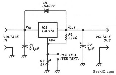
The variable voltage regulator lets you adjust the output voltage of a fixed dc power supply between 1.2 and 37 Vdc, and will supply the output current in excess of 1.5 A. The circuit incorporates an LM117K three-terminal adjustable output positive voltage regulator in a TO-3 can. Thermal overload protection and short-circuit current-limiting constant with temperature are included in the package. Capacitor C1 reduces sensitivity to input line impedance, and C2 reduces excessive ringing. Diode CR1 prevents C2 from discharging through the IC during an output short, (View)
View full Circuit Diagram | Comments | Reading(2932)
| Pages:889/2234 At 20881882883884885886887888889890891892893894895896897898899900Under 20 |
Circuit Categories
power supply circuit
Amplifier Circuit
Basic Circuit
LED and Light Circuit
Sensor Circuit
Signal Processing
Electrical Equipment Circuit
Control Circuit
Remote Control Circuit
A/D-D/A Converter Circuit
Audio Circuit
Measuring and Test Circuit
Communication Circuit
Computer-Related Circuit
555 Circuit
Automotive Circuit
Repairing Circuit