
Circuit Diagram
Index 897
ELECTRONIC_ROULETTE_GAME
Published:2009/7/9 4:36:00 Author:May

R14 is set for an initial starting speed of the oscillator U1A and U1B. As C2 charges, oscillation begins slowing down as C2 discharges, giving a roulette-wheel effect on LED S1 through 10. The LED that remains on is the winning number. (View)
View full Circuit Diagram | Comments | Reading(1582)
CAPACITOR_DISCHARGE_HIGH_VOLTAGE_GENERATOR
Published:2009/7/9 4:36:00 Author:May

Stepdown transformer T1 drops the incoming line voltage to approximately 48 Vac which is rectified by diode D1; the resultant dc charges capacitor C1-through current limiting resistor R1-to a volt-age level preset by R4. When the voltage on R4's wiper reaches about 8.6 V, Q1 begins to turn on, drawing current through R7 and the base-emitter junction of Q2. Q2 turns on and supplies a positive voltage to the gate of silicon-controlled rectifier Q3. The positive gate voltage causes Q3 to conduct, thereby discharging C1 through the primary winding of step-up transformer T2, which results in a high-voltage arc at output terminal X. The voltage developed at T2's output is determined by the value of C1, the voltage across Q1, and the turns ratio of transformer T2. The frequency or pulse rate of the high voltage is determined by the resis-tance of T1's primary and secondary windings, the value of R1, and the value of C1. The lower the value of each item, the higher the output pulse rate ; the peak output voltage will only remain unchanged if C1's value remains unchanged. (View)
View full Circuit Diagram | Comments | Reading(642)
HIGH_VOLTAGE_REGULATOR
Published:2009/7/9 4:34:00 Author:May

The regulator delivers 100-V at 100 mA and withstands shorts to ground。Even at 100 V output,the LT317A functions in the normal mode,maintainting 1.2 C between its output and adjustment pin.Under these conditions, the 30-V zener is off and Q1 conducts.When an output short occurs, the zener conducts, forcing Q1's base to 30 V. This causes Q1's emitter to clamp 2 VBES below VZ, well VIN-VOUT rating of the regulator.Under these conditions,Q1,a high-voltage device,sustains 90 V- VCE at whatever current the transformer specified saturates at 130 mA,while Q1 safely dissipates 12 W.If Q1 and the LT317A are thermally coupled, the regulator will soon go into thermal shutdown and oscillation will commence,This action will continue, protecting the load and the regulator as long as the output remalns shorted.The 500-pF capacitor and the 10 Ω/0.02 μF damper aid transient response and thediodes provide safe discharge paths for the capacitors. (View)
View full Circuit Diagram | Comments | Reading(1203)
NANOAMMETER
Published:2009/7/9 4:34:00 Author:May

Programmable amplifier operating from ±1.5 V supply such as D cells is used as current-to-voltage convener. Offset null of A1 is used to minimize input offset voltage enor. If programmed for low bias current, amplifier can convert currents as small as 100 nA with less than 1% error,Resistor values for variety of current and voltage ranges are give in tables. Adjust R1 to calibrate meter, and adjust R2 to null input offset voltage on lowest range.Not suitable for higher current ranges because power drain is excessive above 100 μA.-W. G. Jung, IC Op-Amp Cookbook, HowardW Sams, Indianapolis, IN, 1974, p 414-417. (View)
View full Circuit Diagram | Comments | Reading(5338)
AUTOMATIC_TURN_OFF_ALARM_WITH_DELAY
Published:2009/7/9 4:34:00 Author:May

In this circuit, IC1A and IC1B act as a monostable multivibrator. Any input from the sensors S1 through S5 forces IC1A to produce logic low, which causes IC1B to turn on Q1 until C3 changes through R6. This action resets the latch formed by IC1A and IC1B. (View)
View full Circuit Diagram | Comments | Reading(641)
TRIAC_UJT_PHASE_CONTROL
Published:2009/7/20 6:22:00 Author:Jessie

Provides wide range of stable control without hysteresis at low outputs and without dependence on supply voltage. Triac eliminates need for transient suppression components that would be required with scr control and permits use of simple two-winding pulse transformer.-M. P. Southworth, Bidirectional Static Switch Simplifies A-C Control, Control Engineering, March 1964, p 75-76. (View)
View full Circuit Diagram | Comments | Reading(819)
REACTION_TIMER
Published:2009/7/9 4:33:00 Author:May

This circuit uses a timer to generate at a 5-ms clock rate.The pulses are shifted into the shift register,one at a time,lighting an LED.An auxiliary timer that generates one pulse per second is used to generate timing to activate the go LED and stare the 5ms pulses clocking into the registers.At the GO signal each player presses his buttons (S3 or S4).The delay (reaction time) is read out on LED4 to LED17;after six seconds,the sequence repeats. (View)
View full Circuit Diagram | Comments | Reading(1311)
1_out_of_32_multiplexer_using_two_IH6116s_and_one_IH5041
Published:2009/7/20 6:23:00 Author:Jessie

1-out-of-32 multiplexer using two IH6116s and one IH5041. The IH6116s are CMOS 16-channel analog multiplexers (courtesy Intersil, Inc.). (View)
View full Circuit Diagram | Comments | Reading(560)
CASCADED_TWO_TUBE_PHASE_SHIFTER
Published:2009/7/20 6:23:00 Author:Jessie

Provides phase shifts well over 180°with highly constant output voltage. Use of tubes in place of transformer gives wide-band operation, from 500 to 2,000 cps.-W. G. Shepard, Phase Shifter Range Exceeds 180°, Electronics, 31:19, p 96-100. (View)
View full Circuit Diagram | Comments | Reading(1479)
CAR_ALARM_WITH_HORN_AS_LOUDSPEAKER
Published:2009/7/9 4:33:00 Author:May

An auto horn will work as a speaker of limited audio-frequency range. This circuit uses a 555 timer as an oscillator to drive an MJE34 transistor, which in turn drives the horn. Normal horn operation is ensured by blocking diode D4. (View)
View full Circuit Diagram | Comments | Reading(914)
2_levei_8_channel_multiplexor
Published:2009/7/20 6:25:00 Author:Jessie

2-levei 8-channel multiplexor (courtesy Motorola Semiconductor Products Inc.). (View)
View full Circuit Diagram | Comments | Reading(581)
AUTO_IGNITION_CUT_OFF
Published:2009/7/9 4:30:00 Author:May

Using an SCR/relay combination, this circuit can be made to cut off ignition, unless a positive voltage is applied to'the gate of the SCR. This is useful as an anti-theft device, because depending on hook-up, the 'car wili not start unless a certain accessory or a hidden switch is closed. (View)
View full Circuit Diagram | Comments | Reading(1143)
AUTO_ALARM
Published:2009/7/9 4:29:00 Author:May

S1 is external key switch. The alarm allows a 0-to 45-s delay after S1 is operated before the circuit is armed. During this period, LED1 lights green. After this delay, LED1 lights red, which indicates that the circuit is armed. Then, sensors S2 through S4 -(NO) or S5 through S6 (NO) pull pin 2 of U2 low, which activates K1 and sounds the alarm. The alarm sounds for a duration determined by R4 and C2. After this time, K1 releases and the circuit is again ready. Manual reset is via the key switch, S1. (View)
View full Circuit Diagram | Comments | Reading(1483)
3_25_V_DC_DC_CONVERTER
Published:2009/7/9 4:26:00 Author:May

View full Circuit Diagram | Comments | Reading(593)
10_watt_UHF_microstrip_amplifier_for_450_to_470_MHz
Published:2009/7/20 7:31:00 Author:Jessie

10-watt UHF microstrip amplifier for 450 to 470 MHz (courtesy Motorola Semiconductor Products Inc.). (View)
View full Circuit Diagram | Comments | Reading(1040)
HIGH_VOLTAGE_INVERTER
Published:2009/7/9 4:25:00 Author:May

The circuit converts a dc voltage (V+) to a high-amplitude square wave in the audio-frequency range. The dual timer, IC2, provides an inexpensive alternative to the traditional transformer for providing complementary base drive to the power transistors, Q1 and Q2. You can convert a 6 to 12 V battery output, for example, to an ac amplitude, which is limited primarily by the power rating of transformer T1. Connect timer IC1 as an oscillator to provide a symmetrical square-wave drive to both inputs of IC2. The timing components, R2 and C1, produce a 2.2-kHz output frequency. By connecting half of IC2 in the inverting mode and the other half in noninverting mode, the timer's outputs alternately drive the two transistors.You can operate the audio-output transformer, T1, as a step-up transformer by connecting it backwards—using the output winding as an input. The transformer delivers an output voltage across RL of 4 × N × V+V pk-pk, where N is the transformer turns ratio. For the circuit shown, the output swing is 100 × V+V pk-pk. (View)
View full Circuit Diagram | Comments | Reading(1074)
80_watt_175_MHz_FM_transmitter_for_125_volt_operation
Published:2009/7/20 7:29:00 Author:Jessie
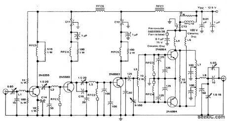

80-watt 175 MHz FM transmitter for 12.5-volt operation. Forthe rated output of 80 watts 180 mW of RF drive is required (courtesy MotorolaJ Semiconductor Products Inc.). (View)
View full Circuit Diagram | Comments | Reading(2391)
HIGH_EFFICIENCY_FLYBACK_VOLTAGE_CONVERTER
Published:2009/7/9 4:25:00 Author:May

U1 is a dual voltage comparator with open collector outputs. The A side is an oscillator operating at 100 kHz, and the B side is part of the regulation circuit that compares a fraction of the output voltage to a reference generated by zener diode D2.The output of U1A is applied directly to the gate of Q1. During the positive half-cycle of the Q1 gate voltage, energy is stored in L1; in the negative half, the energy is discharged into C2. A portion of the output voltage is fed back to U1B to provide regulation. The output voltage is adjustable by changing feedback potentiometer R9.Using the component values shown will produce a nominal 300-V output from a 12-V source. However, the circuit maximum output voltage is limited by R10; a lower value for R10 yields a higher output voltage. The output voltage is also limited by the breakdown of values Q1, L1, D1, and C2. (View)
View full Circuit Diagram | Comments | Reading(1048)
AUTO_TURN_OFF_ALARM_WITH_8_MINUTE_DELAY
Published:2009/7/9 4:24:00 Author:May

This circuit uses a NE555 timer and CD4020B. When + 12 Vdc is applied to the circuit, the output of IC2 is set low via C2, which turns on the relay, and IC1, a pulse generator. IC1 pulses counter IC2. After 8192 clocks, IC2 output (pin 3) goes high, cuts off Q2, and completes the cycle. (View)
View full Circuit Diagram | Comments | Reading(591)
Single_stage_80_watt_RF_power_amplifier_for_144_to_175_MHz_FM_operation
Published:2009/7/20 7:26:00 Author:Jessie
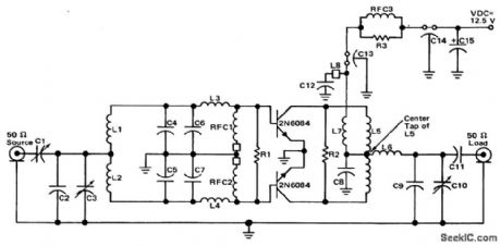

Single-stage 80-watt RF power amplifier for 144 to 175 MHz FM operation. About 25 watts of drive are required for the rated output (courtesy Motorola Semiconductor Products mc.). (View)
View full Circuit Diagram | Comments | Reading(1806)
| Pages:897/2234 At 20881882883884885886887888889890891892893894895896897898899900Under 20 |
Circuit Categories
power supply circuit
Amplifier Circuit
Basic Circuit
LED and Light Circuit
Sensor Circuit
Signal Processing
Electrical Equipment Circuit
Control Circuit
Remote Control Circuit
A/D-D/A Converter Circuit
Audio Circuit
Measuring and Test Circuit
Communication Circuit
Computer-Related Circuit
555 Circuit
Automotive Circuit
Repairing Circuit