
Circuit Diagram
Index 899
200_MHz_RF_amplifier_using_the_ECG703A_10_
Published:2009/7/20 6:58:00 Author:Jessie
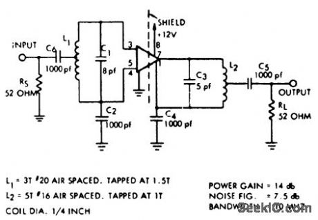
200 MHz RF amplifier using the ECG703A 10 (courtesy of GTE Sylvania Incorporated). (View)
View full Circuit Diagram | Comments | Reading(887)
LIGHT_METER_WITH_LED_READOUT
Published:2009/7/9 4:23:00 Author:May

Light onphototransistorQ1 (Radio Shack 276-130) produces voltage change across R2 for amplification by opamp whose output drives array fiveLEDs forming bar graph voltage indicator. Adjust R3 initially for highest sensitivity by tuming off room lights and rotating until LED 1 just stops glowing. Now, as light is gradually increased on sensor, LEDs come on one by one in upward sequence and stay on until all five are lit. Solar cells or selenium cells can be used in place of phototransistor.-F. M. Mims, Opto-electronic Projects, Vol. 1, Radio Shack, Fort Worth, TX, 1977, 2nd Ed., p 85-93. (View)
View full Circuit Diagram | Comments | Reading(1472)
30_MHz_PF_amplifier_with_transformer_coupling_using_the_EOG703A_
Published:2009/7/20 6:57:00 Author:Jessie
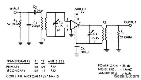
30 MHz PF amplifier with transformer coupling using the EOG703A (courtesy GTE Sylvania Incorporated). (View)
View full Circuit Diagram | Comments | Reading(909)
BACKUP_BEEPER
Published:2009/7/9 4:22:00 Author:May

When the vehicle's backup lights kick on, or when the manual switch (S1) is closed, a small current is fed to the base of Q1. Transistor Q1 allows current to flow through it and, if the enable switch (S2) is closed, it sends 12 V to UI, a 555 timer. Timer UI sends high pulses that last 0.97713 s and low signals that last 0.488565 s to the base of Q2. When UI switches Q2 on, it sends 12 V to BZ1, a piezoelectric buzzer. For best results, the buzzer should be mounted under the vehicle-somewhere where people around the car can hear the warning beeps. (View)
View full Circuit Diagram | Comments | Reading(830)
SIMPLE_HIGH_VOLTAGE_SUPPLY
Published:2009/7/9 4:21:00 Author:May

This circuit can generate high-voltage pulses with an inexpensive auto ignition coil. Add a rectifier on the output and the circuit produces high-voltage dc. The circuit's input is 115 Vac. During the input's positive half cycle, energy is stored in capacitor C1, which is charged via diode D1 and the primary winding of transformer T1, the coil. The SCR and its trigger circuitry are inactive during this period. During the input's negative half cycle, energy is stored in capacitor C2 until diac D2 reaches its trigger voltage, whereupon D2 conducts abruptly and C2 releases its energy into the SCR's gate. The SCR then discharges C1 into the transformer's primary and ceases to conduct. This store-and-release cycle repeats on the line's positive and negative half cycles, producing high-voltage pulses at the transformer's secondary. (View)
View full Circuit Diagram | Comments | Reading(0)
PHASE_INDICATOR
Published:2009/7/20 6:56:00 Author:Jessie

Used to determine succession of phases of three phase 120-V a-c source used in synchro work. Terminals A, B, and C are connected to terminals of source to be checked. If neon lamp comes on, interchange any two leads; light then goes out, and A, B, and C then indicate correct sequence. Also serves as phase failure monitor, because neon lamp will come on if power on any one line is lost.-G. Richwell, Phase Indicator, EEE, 12:11, p 70. (View)
View full Circuit Diagram | Comments | Reading(0)
EFFICIENT_SUPPLY_SPLITTER
Published:2009/7/9 4:20:00 Author:May

In this application, the VI-7660 is connected as a voltage splitter. Note that the normal output pin is connected to ground and the normal ground pin is used as the output. The switches that allow the charge pumping are bidirectional; therefore, charge transfer can be performed in reverse. The 1-MΩ resistor is used to avoid start-up problems by forcing the internal regulator on. An application for this circuit would be driving low-voltage, ±7.5 Vdc, circuits from ±15 Vdc supplies, or low-voltage logic from 9 to 12 V batteries. (View)
View full Circuit Diagram | Comments | Reading(603)
25_watt_AM_transmitter_designed_for_118_MHz_to_136_MHz_operation
Published:2009/7/20 6:55:00 Author:Jessie

2.5-watt AM transmitter designed for 118 MHz to 136 MHz operation (courtesy Motorola Semiconductor Products Inc.). (View)
View full Circuit Diagram | Comments | Reading(2069)
AUTOMATIC_ARMING_AUTO_ALARM
Published:2009/7/9 4:20:00 Author:May

The circuit automatically turns on when the car is turned off. It gives you a variable time to get out and lock up, and also provides a variable time delay to get in and start the car.
The 555 oscillator/timers are always powered down when the car is on. That keeps the alarm from going off while you're driving. As soon as the car is turned off, Q2 switches off and shunts power to U1. When that happens, U1 immediately sends its output high, keeping Q3 on, and thereby prevents power from returning to U2.
Transistor Q2 also sends power to Q3's collector to be used only when U1 has completed its timing cycle. When U1 has finished, it turns Q3 off, which in turn activates Q4, and sends power to the balance of the circuit. That timing period was the time needed to get out of the car. LED1 indicates that the system is disarmed and LED2 indicates that the system is armed.
At this point, U2 whits for a trigger pulse from the car's door switches or dome light. A positive impulse at the 4011's input sends a negative trigger pulse to the first stages of U2, which is connected as a cascading timer. The first stage's output becomes high for a time to allow the car to be turned on.
If that does not happen, the first stage's output lowers, which sends a low trigger pulse to the second stage. The second stage then sends its output high, turning on Q5, which sounds the alarm for a given time. Once that time has elapsed, the alarm is shut off by a low output to Q5 and the system is reset. If the car door is closed or a second door opened while the alarm is sounding, the first stage retriggers and pre-pares to extend the ON-time of the alarm.
The cascading or counting action continues until the car is left alone. You can add a switch on the positive supply rail at J3 to override and silence the alarm, if (for example) you plan to work on the car.Switch S1 is a normally closed type that is built into the case of the alarm; S1 is pushed to the open posi-tion when the case is mounted flush with a surface. Any attempt to remove the alarm will sound the alarm. (View)
View full Circuit Diagram | Comments | Reading(729)
OPTOISOLATED_HIGH_VOLTAGE_DRIVER
Published:2009/7/9 4:19:00 Author:May

This circuit takes as an input a signal from a 5-V CMOS logic circuit and outputs a high voltage of the same polarity. The high-voltage supply can be varied from (30 V to ) 150 V without the need to change circuit components. The input voltage is applied to the gates of transistors TR1 and TR2.TR3 is optically coupled to D1 as is TR5 to D2. R5 limits the current through D2, while R3 and R4 reduce the affects of leakage current. The light transmitted by D1 turns TR3 on and discharges the gate-source capacitance of TR6, which turns TR6 off. At the same time, TR5 is off and a constant current produced by R6, R7, D3, and TR4 charges the gate-sourced capacitance of TR7, thus turning TR7 on.With TR7 on and TR6 off, the output is pulled close to the lower supply rail. When the input is high, TR1 is off and TR2 is on. Therefore, D2 conducts, which turns on TR5. With TR3 off and TR5 on, TR6 turns on and TR7 off. The output is pulled towards the higher supply rail. (View)
View full Circuit Diagram | Comments | Reading(727)
PULSE_TRAIN
Published:2009/7/9 4:19:00 Author:May
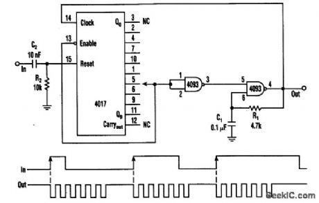
This circuit has a rate multiplier usmg a 4093 Schmitt trigger as an oscillator,driving a 4017 decadecounter. When a pulse present at the input(to C2)4017 is reset,output zero goes high,and outputs 1 to 9 go low.The oscillator(4093)starts runrung and the 4017 counts the pulses until the 4017 output(1 to 9)connected to pin 1 and 2 of the 4093 goes high.The osciffator IS inhibited and the output remains high until the next input pulse. (View)
View full Circuit Diagram | Comments | Reading(2890)
UNIPOLAR_TO_DUAL_SUPPLY_CONVERTER
Published:2009/7/9 4:17:00 Author:May

The outputs in this circuit are independently variable and can be loaded unsymmetrically. The output voltage remains constant, irrespective of load and changes. By varying potentiometers R2 or R6, the output voltages can be conveniently set. Outputs can be varied between 8 and 17 V, so that the standard ±9, ±12, and ±15 V settings can be made. This converter is designed for a maximum load current of 1 A and the output impedance of both supplies of 0.35 Ω. This circuit is not protected against shortcircuits, but Uses the protection provided by the dc input source. This circuit is ideal for biassing operation amplifier circuits. (View)
View full Circuit Diagram | Comments | Reading(603)
BATTERY_POWERED_HIGH_VOLTAGE_GENERATOR
Published:2009/7/9 4:17:00 Author:May
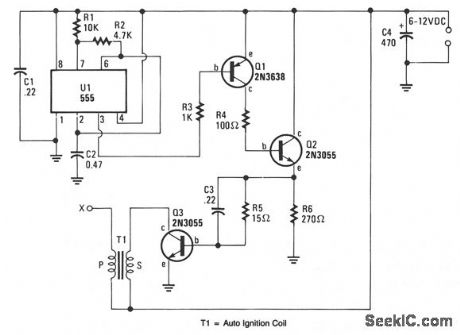
Output voltage great enough to jump a 1-inch gap can be obtained from a 12-V power source. A 555 timer IC is connected as an astable multivibrator that produces a narrow negative pulse at pin 3. The pulse turns Q1 on for the duration of the time period. The collector of Q1 is direct-coupled to the base of the power transistor Q2, turning it on during the same time period. The emitter of Q2 is direct-coupled through current limiting resistor R5 to the base of the power transistor. Q3 switches on, producing a minimum resistance between the collector and emitter. The high-current pulse going through the primary of high-voltage transformer T1 generates a very high pulse voltage at its secondary output terminal (labeled X). The pulse frequency is determined by the values of R1, R2, and C2. The values given in the parts list were chosen to give the best possible performance when an auto-ignition coil is used for T1. (View)
View full Circuit Diagram | Comments | Reading(998)
FREQUENCY_RATIO_MONITORING_CIRCUIT
Published:2009/7/9 4:15:00 Author:May
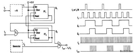
This circuit produces an output frequency that is linearly proportionj to the ratio oftwo input frequen-cies fl/f2.Each pulse of the bias f1(or f)will open G1 for a period T=1/f2 so that fg/f2, pulses pass to the output. (View)
View full Circuit Diagram | Comments | Reading(648)
VARIABLE_0_180_DEG_PHASE_SHIFTER
Published:2009/7/20 6:54:00 Author:Jessie
Single low-cost pnp germanium transistor circuit gives any desired phase between 0 and 180 degrees, at constant amplitude, for frequencies up to 3 Mc, by varying values of C2 and R5. Values shown gives 90° shift for 200 cps. –J. J. Collins, Single Transistor Provides Low-Cost Phase Shifter, Electronics, 37:16, p 92. (View)
View full Circuit Diagram | Comments | Reading(2411)
SIX_RANGE_LIGHT_METER
Published:2009/7/9 4:15:00 Author:May

Switching of feedback resistors for opamp driven by Radio Shack 276-115 selenium solar cell gives multirange linear light meter. With 1000-megohm resistor for highest sensitivity, star Sirius will produce pho-tocurrent of about 25 pA when aolar cell is shielded from ambient light with length of cardboard tubing. Supplies are 9 V, and meter is 0-1 mA.-F. M. Mims, Integrated Circuit Projects, Vol. 4, Radio Shack, Fort Worth, TX, 1977, 2nd Ed., p 45-53. (View)
View full Circuit Diagram | Comments | Reading(3251)
Two_stage_60_MHz_IF_amplifier_with_power_gain_of_80_dB_and_bandwidth_of_15MHz
Published:2009/7/20 6:53:00 Author:Jessie
Two-stage 60 MHz IF amplifier with power gain of 80 dB and bandwidth of 1.5MHz (courtesy Motorola Semiconductor Products Inc.). (View)
View full Circuit Diagram | Comments | Reading(1103)
DIGITAL_MISCELLANEOUS_TEMPERATURE_GAUGE
Published:2009/7/9 4:15:00 Author:May

A diode (IN4148) is used as a temperature sensor. IC2 is an A/D converter with BCD output. A reference voltage set by R7 is applied to the positive input of IC2. As the temperature increases, the voltage across the temperature sensor resistance decreases. This increases the differential input voltage across pins 10 and 11 of IC2. R3 adjusts low calibration. R17 zeros the A/D converter and R7 adjusts high calibration. (View)
View full Circuit Diagram | Comments | Reading(1667)
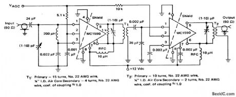
100_MHz_mixer_using_an_MC1590_BF_IF_amplifier
Published:2009/7/20 6:52:00 Author:Jessie

100 MHz mixer using an MC1590 BF-IF amplifier (courtesy Motorola Semiconductor Products Inc.). (View)
View full Circuit Diagram | Comments | Reading(1399)
HIGH_VOLTAGE_DC_GENERATOR
Published:2009/7/9 4:14:00 Author:May

This circuit is fed from a 12-Vdc power supply.The input to the circuit is then amplified to providea 10, 000-Vdc output.The output of the up-converter is then fed into a 10 stage, high-voltage multiplier to produce an output of 10, 000 Vdc. (View)
View full Circuit Diagram | Comments | Reading(0)
| Pages:899/2234 At 20881882883884885886887888889890891892893894895896897898899900Under 20 |
Circuit Categories
power supply circuit
Amplifier Circuit
Basic Circuit
LED and Light Circuit
Sensor Circuit
Signal Processing
Electrical Equipment Circuit
Control Circuit
Remote Control Circuit
A/D-D/A Converter Circuit
Audio Circuit
Measuring and Test Circuit
Communication Circuit
Computer-Related Circuit
555 Circuit
Automotive Circuit
Repairing Circuit