
Circuit Diagram
Index 886
FEEDBACK_OPAMP_FOR_BRIDGE
Published:2009/7/9 5:55:00 Author:May

Uses CA3094 programmable opamp to convert differential input signal from resistor bridge to single-ended 1-V output signal. Circuit provides feedback for opamp. RC network between terminals 1 and 4 of opamp provides compensation to improve stability. - Circuit Ideas for RCA Linear ICs, RCA Solid State Division, Somerville, NJ, 1977, p 13. (View)
View full Circuit Diagram | Comments | Reading(636)
3_digit_ISUP2_SUP_L_A_D_converter_with_LED
Published:2009/7/20 4:43:00 Author:Jessie

3-digit I2 L A/D converter with LED (courtesy Analog Devices, Inc.). (View)
View full Circuit Diagram | Comments | Reading(2258)
IR_RECEIVER_II
Published:2009/7/9 5:51:00 Author:May

Q3 is an IR phototransistor that responds to a modulated IR beam. Q1 amplifies the ac component of the IR beam. Q2 drives a meter as a relative indication of the strength of the light beam. A strong beam gives a lower meter reading. U1 is a tone decoder that produces a low output on pin 1 during reception for an IR beam that is modulated with the correct tone frequency, determined by R6. (View)
View full Circuit Diagram | Comments | Reading(1090)
2_watt_AF_power_amplifier_with_8_ohm_load_connected_to_ground
Published:2009/7/20 4:43:00 Author:Jessie

2-watt AF power amplifier with 8-ohm load connected to ground. Rated output of 2 watts is obtained with a power supply voltage of 12 volts. At 9 volts with the same load a rated output of 1.2 watts is obtained. With a 4-ohm load at 9 volts 1.6 watts is obtained. Capacitor C6 must be used when high ripple rejection is required. The ECG1117 is a 14-pin QIP (courtesy GTE Sylvania Incorporated). (View)
View full Circuit Diagram | Comments | Reading(682)
25_V_D_C_REGULATOR
Published:2009/7/20 4:43:00 Author:Jessie

Provides up to 1.5 amp at 25 v with l% regulation for inputs of 26 to 50 v from unregulated source. Aux. iliary source Ea must be minimum of 5 v.-NBS, Handbook Preferred Circuits Navy Aeronautical Electronic Equipment, Vol. 11, Semiconductor Device Circuits, PSC 3, p 3.2. (View)
View full Circuit Diagram | Comments | Reading(679)
THREE_STAGE_OPAMP
Published:2009/7/9 5:51:00 Author:May

Responds to difference between two applied signals. Differential output voltage of LM102 pair is applied to balanced differential input of LM107 opamp. 0utput can be metered or used in any other desired manner. Voltage gain is equal to ratio R4/R2 and is 100 for values shown.-E. M. Nol!, Linear IC Principles, Experiments, and Projects, Howard W. Sams, Indianapolis, IN, 1974, p 126. (View)
View full Circuit Diagram | Comments | Reading(950)
VOLTAGE_VARIABLE_90_MC_OSCILLATOR
Published:2009/7/20 4:42:00 Author:Jessie

Ceramic triode in 18-Mc crystal stage has high short-term stability, yet can be pulled about 2 kc by voltage-variable capacitor C1. Fifth harmonic is amplified and buffered for use in measuring phase differences between two signals.-R. T. Stevens, Precision Phase-meter for CW or Pulsed UHF, Electronics, 33:10, p 54-57. (View)
View full Circuit Diagram | Comments | Reading(616)
PLL_DETECTOR_FOR_ALL_METALS
Published:2009/7/9 5:46:00 Author:May

Frequency change produced in Colpitts oscillator by metal object near tank coil is indicated by 565 PLL connected asfrequency meter. Oscillator frequency increases when search coil is brought near nonferrous metal object. Oscillator frequency decreases, as indicated by lower meter reading, when coil is brought nearferrous object.-Signetics Analog Data Manual,''Signetios,Sunnyvale,CA,1977,p 856-858. (View)
View full Circuit Diagram | Comments | Reading(4488)
F_V_convener_with_input_diode_protection_against_high_voltage_transients
Published:2009/7/20 4:42:00 Author:Jessie

F/V convener with input diode protection against high-voltage transients. Model 451 has a 0 to 10 kHz full scale input range and model 453 has a 0 to 100kHz full scale input range. Pins 8 and 9 are the output. Maximum input is ±10 volts (courtesy Analog Devices, Inc.). (View)
View full Circuit Diagram | Comments | Reading(811)
1_HZ_TO-125_MHZ_VOLTAGE_TO_FREQUENCY_CONVERTER
Published:2009/7/9 5:46:00 Author:May
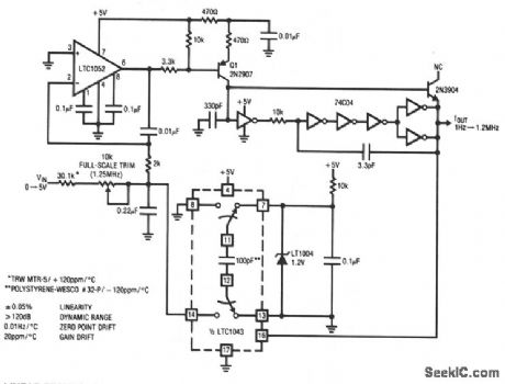
This stabilized voltage-to-frequency converter features 1 Hz-1.25 MHz operation, 0.05% linearity, and a temperature coefficient of typically 20 ppm/°C. This circuit runs from a single 5-V supply. The converter uses a charge feedback scheme to allow the LTC1052 to close a loop around the entire circuit, instead of simply controlling the offset. This approach enhances linearity and stability, but introduces the loop's settling time into the overall voltage-to-frequency step-response characteristic.
(View)
View full Circuit Diagram | Comments | Reading(733)
12_V_BATTERY_CHARGER
Published:2009/7/9 5:44:00 Author:May

This simple charger uses an LM350 regulator as a battery charger. (View)
View full Circuit Diagram | Comments | Reading(0)
IR_RECEIVER_I
Published:2009/7/9 5:44:00 Author:May
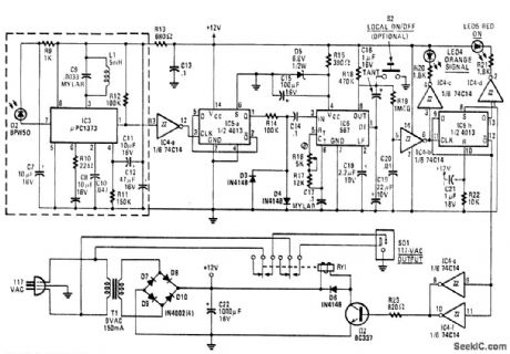
This receiver is built around a μPC1373 IR remote-control preamplifier, a sensitive 30-to-40 kHz tuned detector, an autoniatic gain control, a peak detector, and an output waveshaping buffer. The demod-ulated signal from the preamp stage is sent to IC4A, a 74C14 Schmitt trigger. The squared-up 1 500-Hz signal is then sent to the clock input of IC5A, half of a 4013 dual D flip-flop. That 750-Hz signal is clipped to approximately 0.7-V p-p by diodes D3 and D4. The clipped signal is then fed to IC6, a 567 tone decoder. The output of that IC goes low whenever the frequency of the signal fed to it is within the lock range of its internal VC0.
When IC6 detects a signal of the proper frequency, pin 8 goes low. The output signal is fed through another Schmitt trigger (IC4B), which drives another D flip-flop, IC5B. Schmitt trigger IC4B also drives IC4C, which in turn drives LED4, SIGNAL, which fights up whenever a signal is received. The Q output of IC5B drives two parallel-connected inverters. IC4C and IC4F turn transistor Q2 on when Q goes low. That transistor energizes the relay; its contacts switch the controlled device on and off. (View)
View full Circuit Diagram | Comments | Reading(929)
CURRENT_LIMITED_6_V_CHARGER
Published:2009/7/9 5:44:00 Author:May

An LM317HV regulator is used as a current-limited charger. If current through R4 exceeds 0.6 A, Q1 is biased on, which pulls the ADJ terminal of the LM317 HV to ground and reduces the battery-charging current. (View)
View full Circuit Diagram | Comments | Reading(3119)
V_F_converter_with_10_kHz_full_scale_output
Published:2009/7/20 4:52:00 Author:Jessie

V/F converter with 10 kHz full scale output.The 450 is a high-performance version of the economy 456(courtesy Analog Devices, Inc.). (View)
View full Circuit Diagram | Comments | Reading(886)
VOLTAGE_TO_FREQUENCY_CONVERTER
Published:2009/7/9 5:42:00 Author:May


This circuit can accept positive or negative or differential control voltages. The output frequency is zero when the control voltage is zero. The 741 op amp forms a current source controlled by the voltage EC to charge the timing capacitor C1 linearly. NE555 is connected in the astable mode, so that the capacitor charges and discharges between 1/3 VCC and 2/3 VCC. The offset is adjusted by the 10-K potentiometer so that the frequency is zero when the input is zero. For the component values shown: f≈ 4.2 EC kHz. If two dc voltages are applied to the ends of R1 and R4, the output frequency will be proportional to the difference between the two voltages. (View)
View full Circuit Diagram | Comments | Reading(3428)
BATTERY_CHARGER
Published:2009/7/9 5:42:00 Author:May

This high-performance charger quickly charges gelled lead-acid batteries, and turns off at full charge. At first, the charge current is held at 2 A, but as battery voltage rises, current decreases. When current falls to 150 mA, the charger automat- ically switches to a lower float voltage to keep from overcharging. When you hit full charge, transistor Q1 lights the LED to indicate that status. (View)
View full Circuit Diagram | Comments | Reading(0)
45_wad_AF_power_amplifier_using_an_ECG1081
Published:2009/7/20 4:52:00 Author:Jessie

4.5-wad AF power amplifier using an ECG1081. Recommended supply voltage is 13.2 volts, which makes it ideal for automotive applications. Voltage gain at 400 hertz is 50 dB (courtesy GTE Sylvania Incorporated). (View)
View full Circuit Diagram | Comments | Reading(576)
HODOSCOPE_AMPLIFIER
Published:2009/7/9 5:41:00 Author:May

Charge amplifier using Teledyne Philbrick 102601 opamp was developed for use with each Geiger counter of 132-counter array for ionization hodoscope used in tracing paths of cosmic rays. Charge-sensitive stage A1 converts input charge pulse tovoltage pulse significantly larger than noise of second stage. With 616-pF load capacitor, output is 12 V for input of 10 mV. Cost of charge amplifier is about $50.-H. C. Carpenter, Low Cost Charge Amplifier, EDN Magazine, May 20, 1973, p 83 and 85. (View)
View full Circuit Diagram | Comments | Reading(4023)
50_V_D_C_REGULATOR
Published:2009/7/20 4:51:00 Author:Jessie

Provides up to 750 ma at 50 v with 1% regulation for inputs of 59 to 100 v from unregulated source. Auxiliary source Ea must be minimum of 5 v.-NBS; Handbook Preferred Circuits Navy Aeronautical Electronic Equipment, Vol. 11, Semiconductor Device Circuits, PSC 4, p 4-2. (View)
View full Circuit Diagram | Comments | Reading(661)
F_V_converter_monitoring_the_60_hertz_line_frequency
Published:2009/7/20 4:51:00 Author:Jessie

F/V converter monitoring the 60-hertz line frequency. The gain of the F/V converter has been set to 0.1 volt per hertz, which results in a100-hertz full scale frequency range (courtesy Analog Devices, Inc.). (View)
View full Circuit Diagram | Comments | Reading(803)
| Pages:886/2234 At 20881882883884885886887888889890891892893894895896897898899900Under 20 |
Circuit Categories
power supply circuit
Amplifier Circuit
Basic Circuit
LED and Light Circuit
Sensor Circuit
Signal Processing
Electrical Equipment Circuit
Control Circuit
Remote Control Circuit
A/D-D/A Converter Circuit
Audio Circuit
Measuring and Test Circuit
Communication Circuit
Computer-Related Circuit
555 Circuit
Automotive Circuit
Repairing Circuit