
Circuit Diagram
Index 884
21_watt_AF_power_amplifier_for_phonographs_tape_recorders
Published:2009/7/20 4:56:00 Author:Jessie

2.1-watt AF power amplifier for phonographs/tape recorders. It is recommended that a 12-volt supply be employed, which makes it ideal for automotive applications. THe ECG1113 is a 14-pin QIP. Current drain at maximum output is 235 mA (courtesy GTE Sylvania Incorporated). (View)
View full Circuit Diagram | Comments | Reading(626)
ACCESS_CONTROL_FOR_OPEN_REPEATER
Published:2009/7/20 4:56:00 Author:Jessie

Permits repeater to run open, for user access without access tone, when there is no outside interference on input frequency. Carrier-operated relay (COR) pulse is shaped by 7400 gates U5A and U5B, for keying transmitter through U5C as long as output of U5D is high. (Turning guard control switch off latches output of U5D high, letting repeater run open) When control switch is on, repeater can be accessed only by use of guarded input applied toQ1 such as 2000-Hz tone burst, 1336-Hz Touch-Tone signal, or 110.9-Hz private line. Repeater then remains open for 5s after duration of each transmission. System prevents fringe-area station from blocking repeater access for local users. When receiver squelch is operated 3 times in succession by signal not having one of access tones, input is automatically guarded for 15min by timer U3-U4 unless accepted access tone arrives.-R. B.Shrove, Troubleshooting Logic Circuits, Ham Radio, Feb, 1977, p 56-59. (View)
View full Circuit Diagram | Comments | Reading(1791)
PREFERRED__150_V_D_C_REGULATOR
Published:2009/7/20 4:55:00 Author:Jessie
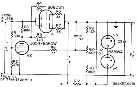
Provides 1% output voltage regulation under normal line and load variations of military equipment. Minimum value of C3 is 2 mfd. Value of R12 depends on reference voltage Er, which should be minimum of -300 v d-c. Two reference tubes, V3 and V4, are used in series so negative bias for V2 can be obtained with grounded reference supply. Minimum input voltage is 200 v d-c.-NBS, Handbook Preferred Circuits Navy Aeronautical Electronic Equipment, Vol. 1, Electron Tube Circuits, 1963, PC 2, p 2-2. (View)
View full Circuit Diagram | Comments | Reading(2835)
The medical constant temperature box (1)
Published:2011/7/21 20:02:00 Author:qqtang | Keyword: constant temperature box

Here is to introduce a medical constant temperature box which is fixed with the temperature sensor integrated circuit, and the temperature control range is -25-+100℃.The working principle of the circuitThe medical constant temperature box consists of the temperature detection amplifier circuit, trigger, control circuit and power supply circuit, see as figure 9-40.
The temperature amplifier circuit consists of the precise regulated integrated circuit IC1, temperature sensor integrated circuit IC2, computing amplifier integrated circuit IC3 (N1 and N2), resistor R1-R5 and resistors RP1 and RP2. (View)
View full Circuit Diagram | Comments | Reading(1176)
12_bit_D_A_multiplying_convener_with_an_AD509_op_amp
Published:2009/7/20 4:55:00 Author:Jessie

12-bit D/A multiplying convener with an AD509 op amp (courtesy Analog Devices, Inc.). (View)
View full Circuit Diagram | Comments | Reading(899)
12_bit_multiplying_D_A_converter_with_an_AD518_op_amp
Published:2009/7/20 4:54:00 Author:Jessie

12-bit multiplying D/A converter with an AD518 op amp (courtesy Analog Devices, Inc.). (View)
View full Circuit Diagram | Comments | Reading(934)
10_bit_D_A_convener_in_unipolar_binary_operation
Published:2009/7/20 4:54:00 Author:Jessie

10-bit D/A convener in unipolar binary operation(courtesy Analog Devices,Inc.). (View)
View full Circuit Diagram | Comments | Reading(827)
1800_Hz_COMMAND_OSCILLATOR
Published:2009/7/20 4:53:00 Author:Jessie

Connects across microphone leads of FM transceiver, to produce control (command) tone for entry to repeater or for other purposes. Switch may be placed in supply lead if desired. Q1 can be 2N404 or one of transistors in 2N1303, 2N2904, 2N3638, 2N6516, or 2N6533 series. Q2 can be 2N1308, 2N2712, 2N3565, 2N3569, 2N6513, or equivalent. CTRIM is 0.0062 μF.-Circuits, 73 Magazine, April1973, p 132. (View)
View full Circuit Diagram | Comments | Reading(2062)
10_bit_D_A_converter_in_bipolar_operation
Published:2009/7/20 4:53:00 Author:Jessie

10-bit D/A converter in bipolar operation (courtesy Analog Devices, Inc.). (View)
View full Circuit Diagram | Comments | Reading(759)
200_V_D_C_TO_24_V_D_C_REGULATED_POWER_SUPPLY
Published:2009/7/20 4:53:00 Author:Jessie

Gate turnoff and silicon power transistor together provide switching and regulating action efficiently at high frequency for d-c/d-c stepdown transformer applications.-D. R. Grafham, Now the Gale Turnoff Switch Speeds Up D-C Switching, Electronics, 37:12, p 64-71. (View)
View full Circuit Diagram | Comments | Reading(660)
1_wat_OTL_AF_power_amplifier_using_an_ECG1126_14_pin_DIP_with_tab_Typical_voltage_gain_is_40_dB
Published:2009/7/20 4:52:00 Author:Jessie

1-wat OTL AF power amplifier using an ECG1126 14-pin DIP with tab Typical voltage gain is 40 dB. Maximum current drain is 35 mA (courtesy GTE Sylvania Incorporated). (View)
View full Circuit Diagram | Comments | Reading(543)
V_F_converter_used_as_a_nearly_18_bit_A_D_converter
Published:2009/7/20 4:52:00 Author:Jessie

V/F converter used as a nearly 18-bit A/D converter. Resolution is 1 pulse in 200,000, or 0.05% of the smallest input signal (courtesy Analog Devices, Inc.). (View)
View full Circuit Diagram | Comments | Reading(736)
13_watt_AF_power_amplifier_using_an_ECG1139_module_and_powered_by_two_16_volt_supplies
Published:2009/7/20 5:02:00 Author:Jessie

13-watt AF power amplifier using an ECG1139 module and powered by two 16-volt supplies. Use a 2-ampere fuse in the output. Voltage gain is 33 dB (courtesy GTE Sylvania Incorporated). (View)
View full Circuit Diagram | Comments | Reading(624)
F_V_and_V_F_converters_used_in_a_two_wire_data_transmission_system_Model_610_instrumentation_amplifier_amplifies_the_low_level_differential_transducer_signal_to_the_10_voltfull_scale_of_models_450_and_456_10_kHz_V_F_conveners
Published:2009/7/20 5:01:00 Author:Jessie

F/V and V/F converters used in a two-wire data transmission system Model 610 instrumentation amplifier amplifies the low-level differential transducer signal to the 10-voltfull scale of models 450 and 456 10 kHz V/F conveners. A differential line driver is used to drive the twisted pair through a noisy environment. A differential line receiver is used to drive model 451 10 kHz F/V converter (courtesy Analog Devices, Inc.). (View)
View full Circuit Diagram | Comments | Reading(834)
12_bit_multiplying_D_A_converter_in_bipolar_operation
Published:2009/7/20 5:00:00 Author:Jessie

12-bit multiplying D/A converter in bipolar operation. In this configuration the converter is set up for four-quadrant multiplication (courtesy Analog Devices Inc.). (View)
View full Circuit Diagram | Comments | Reading(749)
TEMPERATURE_STABILIZED_1_TO_17_V
Published:2009/7/20 4:59:00 Author:Jessie

Shunttype supply uses prestabilizer to control temperature controller and stabiilzing circuit that serves as voltage reference. After reaching equilibrium temperature in 5 hours, overall drift over 15-hour period is only 36 microvolts per hour at 6 v output. Ripple voltage is 0.1 my maximum peak-to-peak.-E. Baldinger and W. Czaja, Designing Highly Stable Transistor Power Supplies, Electronics, 32:39, p 70-73. (View)
View full Circuit Diagram | Comments | Reading(535)
FIRING_ANGLE_CONTROL
Published:2009/7/20 4:59:00 Author:Jessie

Varying R from 0 to infinity shifts the three phase voltages from 0° to 180°.-J. J. Vithayathil, Variable-Phase, Polyphase From Single-Phase Supply, Electronics, 37:27, p 56-57. (View)
View full Circuit Diagram | Comments | Reading(608)
IR_CONTROLLED_SOLDERING_STATION
Published:2009/7/9 20:35:00 Author:May

An IR-sensitive phototransistor is used to sense soldering-iron temperature. The phototransistor must see the tip through an opaque tube to avoid stray light, and the phototransistor should preferably be fitted with an IR filter. An old photo negative, dark red plastic, or red or black glass can be used. The iron sits on a holder.
When the iron is removed from the holder, the iron is not being viewed by the detector. The heat will increase, but the circuit has a lag time; if the iron is returned to its holder after each use, overheating should not be a problem. (View)
View full Circuit Diagram | Comments | Reading(3067)
12_bit_multiplying_D_A_convener_in_unipolar_operation
Published:2009/7/20 4:59:00 Author:Jessie

12-bit multiplying D/A convener in unipolar operation. In this configuration the convener is set up for two-quadrant multiplication (courtesy Analog Devices, Inc.). (View)
View full Circuit Diagram | Comments | Reading(710)
DIGITAL_LOGIC_PROBE
Published:2009/7/9 20:33:00 Author:May

The probe relies on the power supply of the CUT (circuit-under-test). The input to the probe, at probe tip, is fed along two paths. One path flows to the clock inputs of U2a and U2b. The other path feeds both the inverting input of U1c, which is set up as an inverting-mode integrator, and the noninverting input of Ulb, which is configured as a noninverting unity-gain amplifier, in a logic-low state.
That low, below the reference set at pin 10, causes U1b's output at pin 7 to become high. With Ub1 outputting low and U1c outputting high, LED1 is forward-biased, and lights. LED2, reverse-biased, remains dark. Suppose that the logic level on the same pin becomes high. That high is applied to pin 5 of Ulb, causing its output to be high. LED2 is now forward,biased and lights, while LED1 is reverse-biased and becomes dark.
Assume that a clock frequency is sensed at the probe input; LED1 and LED2 alternately light, and depending on the frequency of the signal, can appear constantly lit. That frequency, which is also applied to the clock input of both flip-flops, causes the Q outputs of U2a and U2b to simultaneously alternate between high and low. Each time that the Q outputs of the two flip-flops decrease, the output of U1d increases, lighting LED3, indicating that a pulse stream has been detected. (View)
View full Circuit Diagram | Comments | Reading(910)
| Pages:884/2234 At 20881882883884885886887888889890891892893894895896897898899900Under 20 |
Circuit Categories
power supply circuit
Amplifier Circuit
Basic Circuit
LED and Light Circuit
Sensor Circuit
Signal Processing
Electrical Equipment Circuit
Control Circuit
Remote Control Circuit
A/D-D/A Converter Circuit
Audio Circuit
Measuring and Test Circuit
Communication Circuit
Computer-Related Circuit
555 Circuit
Automotive Circuit
Repairing Circuit