
Circuit Diagram
Index 890
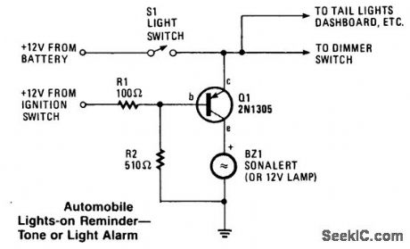
AUTOMOBILE_LIGHTS_ON_REMINDER
Published:2009/7/9 5:07:00 Author:May

The circuit can be used to give a visible or an audible warning that the headlights are on. It uses a 2N1305 transistor as a switch to tum on a Sonalert tone generator or a small 12-V lamp. Operating current for the transistor is supplied from the wire that feeds the headlights. When the ignition is on, the transistor is biased off and the alarm is not activated. Turning off the ignition while the lights are on sets off the alarm. (View)
View full Circuit Diagram | Comments | Reading(824)
Low_power_10_bit_CMOS_D_A_converter_with_10_volt_reference
Published:2009/7/20 4:34:00 Author:Jessie

Low-power 10-bit CMOS D/A converter with 10-volt reference(courtesy Analog Devices, Inc.). (View)
View full Circuit Diagram | Comments | Reading(846)
SIMPLE_UTILITY_MIXER
Published:2009/7/9 5:07:00 Author:May
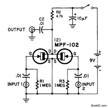

Here's an interesting mixer circuit. With it you can effectively combine signals from audio to high-fre-quency RF. Also, as a special bonus, this circuit will provide some gain at a low noise figure. The inputs can be of almost any level or impedance, and the output (low-Z) will drive most tuned circuits or transistors.Basically, the device consists of two similar FET amplifier stages with a common load resistor (R2). Each FET develops a signal across this resistor, a form of cancellation occurs, and a difference signal results.If you want less gain, try reducing R2 to 2200-Ω. This modification will not affect the mixing ability.
(View)
View full Circuit Diagram | Comments | Reading(1955)
I_F_converter_using_a_V_F_converter_chip
Published:2009/7/20 4:33:00 Author:Jessie

I/F converter using a V/F converter chip. Full scale output is 10 kHz for the 450 and 456 and 20 kHz for the 454 (courtesy Analog Devices, Inc.). (View)
View full Circuit Diagram | Comments | Reading(760)
LIGHTS_ON_REMINDER_FOR_AUTOS
Published:2009/7/9 5:06:00 Author:May

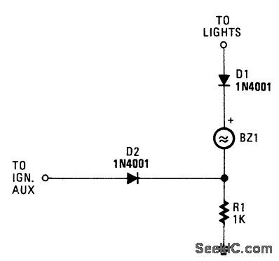
When ignition is off, BZ1 will sound if the head-lights are on. With the ignition on, BZ1 receives no voltage. (View)
View full Circuit Diagram | Comments | Reading(552)
V_F_converter_for_driving_high_noise_immunity_logic_and_CMOS
Published:2009/7/20 4:32:00 Author:Jessie

V/F converter for driving high-noise-immunity logic and CMOS. Full scale output is 10 kHz for the 450 and 456 and 20 kHz for the 454(courtesy Analog Devices, Inc.). (View)
View full Circuit Diagram | Comments | Reading(728)
2_watt_AF_power_amplifier_with_8_ohm_load_connected_to_supply
Published:2009/7/20 4:32:00 Author:Jessie
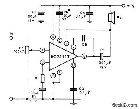
2-watt AF power amplifier with 8-ohm load connected to supply. Rated output of 2 watts is obtained with a supply voltage of 12volts with an 8-ohm load. At 9volts with the same 8-ohm load a rated output of 1.2 watts is obtained. At 9 volts with a 4-ohm load power output is rated at 1.6 watts. Capacitor 06 must be used when high ripple rejection is required. The ECG1117 is a 14-pin QIP (courtesy GTE Sylvania Incorporated). (View)
View full Circuit Diagram | Comments | Reading(504)
DIFFERENTIAL_INPUT_VARIABLE_GAIN
Published:2009/7/9 5:05:00 Author:May

Gainof A3 is varied by modifying feedback returned to R4.A4serves as active attenuator in feedback path presenting constant zero-impedancesource to R4 as required for maintaining goodbalance and high CMRR,With values shown,galn can be varied from unitγ to 300-.W.G.Jung,IC Op-Amp Cookbook,''Howard W,Sams,Indianapolis,IN,1974,ρ 238-239. (View)
View full Circuit Diagram | Comments | Reading(605)
PREFERRED_01_REGULATION_300_V_D_C
Published:2009/7/20 4:32:00 Author:Jessie

Provides either polarity, for applications requiring superior regulation and long-time stability Minimum input is 340 v d-c, and -minimum Esg is 150 v. Maximum load current is 100 ma per series tube. C4 is minimum of 4 mfd.-NBS, Handbook Preferred Circuits Navy Aeronautical Electronic Equipment, Vol. 1, Electron Tube Circuits, 1963 PC 5, p 5-2. (View)
View full Circuit Diagram | Comments | Reading(547)
3_30_V_UNIVERSAL_POWER_SUPPLY_MODULE
Published:2009/7/9 5:05:00 Author:May

U1, an LM317 adjustable regulator provides short-circuit protection and automatic current limiting at 1.5 A. The input voltage to the regulator is supplied by DB1, a 4-A 100 PIV full-wave bridge rectifier. Capacitor C1 provides initial filtering. U1 provides additional electronic filtering as part of the regulating function. The output level of the regulator is set by trimpot R1. Bypass capacitors on the input and output of U1 prevent high-frequency oscillation. The current rating of the transformer must be at least 1.8 times the rated continuous-duty output of the supply. This means that a 1.5-A supply should use a 2.7-A transformer. For light or intermittent loads, a smaller 2.0-A transformer should suffice.Wiring a second LM317, U2, in parallel with U1 is a quick and clean way to increase the current-limiting threshold to 3 A without sacrificing short-circuit protection. When more than 3 A is required, the regulator module can be used to drive the base of one or more pass-transistors (see Fig. 75-2B).
A simple battery-powered switching regulator provides 5 V out from a 9-V source with 80% efficiency and 50 mA output capability. When Q1 is on, its collector voltage rises, forcing current through the inductor. The output voltage rises, causing A1's output to rise. Q1 cuts off and the output decays through the load. The 100-pF capacitor ensures clean switching. The cycle repeats when the output drops low enough for A1 to turn on Q1. The 1-μF capacitor ensures low battery impedance at high frequencies, preventing sqg during switching. (View)
View full Circuit Diagram | Comments | Reading(1485)
REFERENCE_OUTPUT_IN_05_V_STEPS
Published:2009/7/20 4:29:00 Author:Jessie

Eight command signals combined in a binary manner provide stable reference output voltage r from -63.5 v to +63.5 v in 0.5-v steps, with regulation of 0.05% for 5% change in input voltage. System uses two independent d-c power supplies, one delivering fixed 20 v and the other from 20 to 83.5 v in 0.5-v in crements.-M. Beebe and J. Miller, Reference. Supply Delivers Half-Volt Increments, Electronics,35:18, p41-43. (View)
View full Circuit Diagram | Comments | Reading(605)
DIFFERENTIAL_INPUT_VOLTAGE_TO_FREQUENCY_CONVERTER
Published:2009/7/9 5:04:00 Author:May

View full Circuit Diagram | Comments | Reading(490)
NIGHT_SAFETΥ_LIGHT_FOR_AUTOS
Published:2009/7/9 5:03:00 Author:May
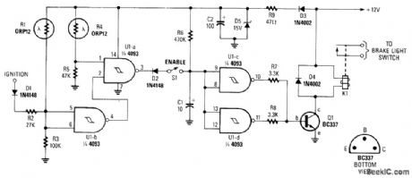
This circuit turns on the brake lights of a parked car when the headlights of an oncoming car are detected, warning the driver of the oncoming car about the parked vehicle. LDR4 is the sensor. LDR1 disables the circuit by causing U1 gate input to be pulled high during daylight hours, causing pin 2 of U1a to become low, disabling it and the circuit. (View)
View full Circuit Diagram | Comments | Reading(1084)
100_kHz_MULTIPLE_OUTPUT_SWITCHING_POWER_SUPPLY
Published:2009/7/9 5:02:00 Author:May


The power supply uses two VN4000A 400-V MOSPOWER FETs in a half-bridge power switch configuration. Outputs availableare+5 V at 20A and±15V or±12 V at 1 A,Since linear three-termlinal regulators are used for the low-current outputs,either±12V or±15V can be made available with a simple change h the transformer secondary windings. A TL494 switching regulator IC provides pulse-width modulation control and drive signals for the power supply.The upper MOSPOWER FET,Q7,In the powerswitch stage is driven by a simple transformer driven by a simple transformer drive circuit.The lower MOS,Q6,smce it is ground referenced,is directly driven fromthe control IC. (View)
View full Circuit Diagram | Comments | Reading(3203)
CAR_HEADLIGHT_CONTROL
Published:2009/7/9 5:01:00 Author:May

It is annoying to realize that you have left your car headlights on only to find that the battery is flat.One possible way to prevent this is with the present control.
The circuit does not provide a warning, but an action: when you switch off the ignition, relay Re1 is de-energized and the headlights are switched off-unless you deliberately decide otherwise. That decision is made possible by switch S1, which, when operated, triggers silicon-controlled rectifier Th1 so that Re1 is nergized. Notice that this is possible only when the ignition switch, S2, is off. Otherwise, the voltage across Th1 is so low, owing to shunt diode Dl, that it cannot be triggered. However, the headlights should not normally be switched on when the ignition is off; in most cases S1 will be used only rarely and the switch can then be omitted altogether. The relay should be a stan-dard 12-V car type with contacts that can switch up to 25 A. (View)
View full Circuit Diagram | Comments | Reading(1108)
MIXER_DIPLEXER
Published:2009/7/9 5:00:00 Author:May
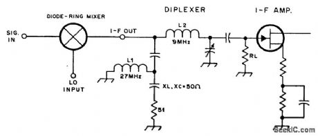
By inserting a high-pass filter section in the IF lead, this mixer is terminated at all frequencies, besides the IF, for other mixer products, which results in improved IMD. In this example, high-pass filter section L1 and capacitors cut off below 28 MHz. Above this frequency, the mixer is terminated.
(View)
View full Circuit Diagram | Comments | Reading(831)
The electromagnet therapeutic apparatus (2)
Published:2011/7/21 20:36:00 Author:qqtang | Keyword: electromagnet, therapeutic apparatus

The working principle of the circuit This electromagnet therapeutic apparatus consists of the ultra-low-frequency oscillator, magnetic pulse generator circuit and power supply circuit, see as figure 9-14.
The ultra-low-frequency oscillator circuit consists of the time-based integrated circuit, resistors R1 and R2, potentiometers C1 and C2, diode VD1 and so on. The magnetic pulse generator circuit consists of the resistor R3, transistor V, diode VD2 and electromagnet coil L. (View)
View full Circuit Diagram | Comments | Reading(1969)
1_Hz_TO_30_VOLTAGE_TO_FREQUENCY_CONVERTER
Published:2009/7/9 4:59:00 Author:May

Circuit has a 1 Hz-to-30 MHz output, 150-dB dynamic range, for a 0 to 5 V input. It maintains 0.08% linearity over its entire 7 1/3 decade range with a full-scale drift of about 20 ppm/°C. To get the additional bandwidth, the fast JFET buffer drives the Schottky TTL Schmitt trigger. The Schottky diode prevents the Schmitt trigger from ever seeing negative voltage at its input. The Schmitt's input voltage hysteresis provides the limits which the oscillator runs between. The 30-MHz, full-scale output is much faster than the LTC1043 can accept, so the digital divider stages are used to reduce the feedback frequency signal by a factor of 20. The remaining Schmitt sections furnish complementary outputs. (View)
View full Circuit Diagram | Comments | Reading(641)
STEREO_LED_VU_METER
Published:2009/7/9 4:59:00 Author:May

This circuit provides a cheap alternative to the LM3915 series LED displays. The meter relies on a square-wave oscillator built around two CMOS analog switches, which alternatively selects the right and left channels for monitoring and display. The selected signal is amplifted by the common-emitter stage T1, and the output is fed into the string comparators which control the display.
These eight comparators are from two LM324 quad op amps, each is connected to a resistor network, which has a 3dB step between each comparator. Each comparator has a positive feedback resistor to increase the hysteresis to provide a longer display, which is switched altematively at about 10 kHz.
The two CMOS switches in line are biased at half the supply voltage by 1-MΩ resistors from a 100-kΩ divider, which allows them to handle analog signals up to 9 V peak to peak. As the voltage increases above the setpoint of each comparator, the output goes low and the corresponding LED lights, which produces a bar of light in response to the input voltage. For a linear response the resistor-network can be replaced by nine 10-kΩ resistors, giving an equal voltage gap before each LED comes on. (View)
View full Circuit Diagram | Comments | Reading(2042)
AUDIO_MIXER
Published:2009/7/9 4:58:00 Author:May
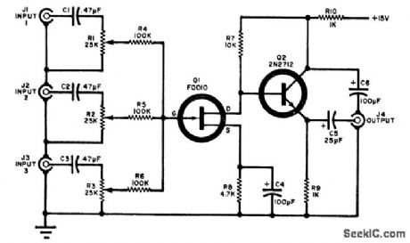
Three audio circuits are combined in the circuit shown. Each input is coupled to its own level potenti-ometer (R1, R2, or R3) and they are combined at the gate of FET Q1. The output of Q1 is coupled to the external audio amplifier through emitter-follower Q2 and capacitor CG. (View)
View full Circuit Diagram | Comments | Reading(0)
| Pages:890/2234 At 20881882883884885886887888889890891892893894895896897898899900Under 20 |
Circuit Categories
power supply circuit
Amplifier Circuit
Basic Circuit
LED and Light Circuit
Sensor Circuit
Signal Processing
Electrical Equipment Circuit
Control Circuit
Remote Control Circuit
A/D-D/A Converter Circuit
Audio Circuit
Measuring and Test Circuit
Communication Circuit
Computer-Related Circuit
555 Circuit
Automotive Circuit
Repairing Circuit