
Circuit Diagram
Index 885
600_mW_AF_power_amplifier_for_a_20_ohm_load
Published:2009/7/20 4:59:00 Author:Jessie

600 mW AF power amplifier for a 20-ohm load. The driver transformer can be purchased locally at Radio Shack (courtesy GTE Sylvania Incorporated). (View)
View full Circuit Diagram | Comments | Reading(559)
CHARGER_EXTENDS_LEAD_ACID_BATTERY_LIFE
Published:2009/7/9 20:32:00 Author:May

The circuit furnishes an initial charging voltage of 2.5 V per cell at 25'C to rapidly charge a battery. The charging current decrbases as the battery charges, and when the current drops to 180 mA, the charging circuit reduces the output voltage to 2.35 V per cell, floating the battery in a fully charged state. This lower voltage prevents the battery from overcharging, which would shorten its life. The LM301A compares the voltage drop across R1 with an 18-mV reference set by R2. The comparator's output controls the voltage regulator, forcing it to produce the lower float voltage when the battery-charging current pass-ing through RI drops below 180 mA. the 150-mV difference between the charge and float voltages is set by the ratio of R3 to R4. The LEDs show the state of the circuit. (View)
View full Circuit Diagram | Comments | Reading(1372)
F_V_converter_controlling_power_load
Published:2009/7/20 4:58:00 Author:Jessie

F/V converter controlling power load. The relay remains open until the preset power on trip level is reached (courtesy Analog Devices, Inc.). (View)
View full Circuit Diagram | Comments | Reading(798)
INFRARED_REMOTE_CONTROLLER
Published:2009/7/9 20:32:00 Author:May

The transmitter is built around two CMOS 555 timer ICs (TLC 555s). The transmitter generates a modulated 35-kHz IR signal. The 35-kHz carrier frequency is generated by IC2, and the 1 500-Hz modu-lating signal is generated by IC1. The output of IC2 drives LED1 through resistor R5; that LED provides visual indication that the transmitter is working. In addition, IC2 drives transistor Q1, which drives the two infrared LEDs (LED 2 and LED3).
To provide the high current needed to drive the two IR LEDs, capacitor C6 is precharged, the charge it contains is dumped when S1 is pressed. When S1 is not pressed, the power to the ICs is cut off. How-ever, C6 is kept charged via R8. Then, when S1 is pressed, the current stored in C6 can be used to drive the LEDs for as much as 1/2 second. That's plenty of time for the receiver to pick up a signal. (View)
View full Circuit Diagram | Comments | Reading(1439)
8_bit_buffered_multiplying_CMOS_D_A_converter_in_bipolar_operation_
Published:2009/7/20 4:58:00 Author:Jessie

8-bit buffered multiplying CMOS D/A converter in bipolar operation (courtesy Analog Devices, Inc.). (View)
View full Circuit Diagram | Comments | Reading(746)
EQUAL_POSITIVE_AND_NEGATIVE_VOLTAGES
Published:2009/7/20 4:58:00 Author:Jessie

Single supply provides equal and opposite output voltages at desired value between 5 and 25 v, at up to 100 ma, for input voltages from 10 to 50 v. R1 balances output voltage, while R2 is adjusted to give good tracking of output voltage.-T. P. Sylvan, Regulator Makes Two Power Supplies Out of One, EEE, 14:5, p 117. (View)
View full Circuit Diagram | Comments | Reading(665)
SENSITIVE_LOW_CURRENT_DRAIN_MOTION_DETECTOR
Published:2009/7/9 20:31:00 Author:May


This highly sensitive movement detector is designed from bipolar transistors and draws a current of only 0.3 mA during quiescent operation. It is intended primarily as a protection device, but it can also be used in certain games.The principle is simple: a magnet is suspended by a thin thread 20 to 30 mm long, and a few millime-ters above the coil of a relay (whose contacts are not used). Even a minute movement of the protectedobject will disturb the magnet. The resulting changes in the magnetic field above the relay coil will induce a tiny varying voltage across the coil.The first stage consists of a common emitter design with automatic regulation. The collector resistors and the resistors in the regulation bridge have unusually high values.Feedback from the bridge ensures stability of operation for T1. Each increase in collector voltage will be opposed by an increase in base-emitter current. Conversely, each reduction in collector voltage will be opposed by a decrease in base-emitter current. Consequently, the collector voltage will stabilize at a value that corresponds to a base voltage of about 0.6 V. Capacitor C1 delays the immediate effect of the feed-back when the collector voltage changes rapidly.The small varying voltage induced in the relay con is magnified appreciably by T1 because C1 prevents automatic regulation. The output impedance of the first stage is very high, which is, of course, the price to be paid for low consumption. It would not make sense to follow this stage by one with a low output impedance, because this would adversely affect the overall amplification. Because of that, T1 is followed by an emitter-follower, T2, which provides the coupling between T1 and T3. Resistor R5 allows a partial discharge of C2 if T2 is switched off by a reduction in the output of T1. Because this resistor, as a result of the low-consump-tion requirement, has a high value, the circuit will attain its maximum sensitivity 10 seconds after the last movement detection. This is the time that is required for the charge on capacitor C2 to stabilize.The detection proper is carried out by T4, which switches on when the voltage variations in the ampli-fier, passed on by C4, reach a level of 0.6 V. Saturating T4 leads to the instant charging of C5. This capaci-tor will discharge partly via R10 and R11 to the base of T5 when T4 switches off again. When C5 dis-charges, T5 is on, which will make T6 conduct. This in turn will actuate a load, for instance, a buzzer, in the collector circuit of T6.The sensitivity of the detector depends to a large extent on the distance between the magnet and relay and the length of the pendulum. If the circuit is powered by a battery, there is a little problem: batteries have large internal resistances.Thus, a supply voltage can vary by some tenths of a volt if a sudden, large current is drawn. If the buzzer has stopped after a detection, such a situation can retrigger the circuit and cause undesired oscillations. To prevent this happening, the supply of the amplifier stage is decoupled by R3 and C6. (View)
View full Circuit Diagram | Comments | Reading(817)
13_watt_AF_power_amplifier_using_an_ECG1137_10_pin_TO_99
Published:2009/7/20 4:58:00 Author:Jessie

1.3-watt AF power amplifier using an ECG1137 10-pin TO-99. Recommended supply voltage is 10 volts and is to be applied across the 470 μF capacitor. Suggested load for the 1.3-watt output is 8 ohms (courtesy GTE Sylvania Incorporated). (View)
View full Circuit Diagram | Comments | Reading(565)
12_bit_multiplying_D_A_converter_with_an_AD741_op_amp
Published:2009/7/20 4:57:00 Author:Jessie

12-bit multiplying D/A converter with an AD741 op amp(courtesy Analog Devices, Inc.). (View)
View full Circuit Diagram | Comments | Reading(1041)
SINGLE_SUPPLY_FAULT_MONITOR
Published:2009/7/9 20:30:00 Author:May

This circuit shows a typical over/under-voltage fault monitor for a single supply. The upper trip points, controlling OUT 1, are centered on 5.5 V with 100 mV of hysteresis (VU = 5.55 V, VL =5.45 V); and the lower trip points, controlling OUT 2, are centered on 4.5 V, also with 100 mV of hysteresis. OUT 1 and OUT 2 are connected together in a wired OR configuration to generate a power Ok signal. (View)
View full Circuit Diagram | Comments | Reading(0)
IR_DETECTOR
Published:2009/7/9 20:29:00 Author:May


Useful for checking TV remote controls, IR-based alarm systems, and IR sources, this circuit causes LED1 to turn on for two seconds in the presence of IR light pulses. U1A acts as a voltage follower for detector Q1. C1 and R2 form a differentiating network and U1B acts as an amplifier for the pulses, which charges C2. Voltage follower U1C samples the voltage on C2 and drives comparator U1D, which switches LED1 on or off.
(View)
View full Circuit Diagram | Comments | Reading(1473)
1_watt_OTL_audio_power_amplifier_with_grounded_load
Published:2009/7/20 4:47:00 Author:Jessie

1-watt OTL audio power amplifier with grounded load. The ECG1097 is a 14-pin DIP with tab (courtesy GTE Sylvania Incorporated). (View)
View full Circuit Diagram | Comments | Reading(588)
+12_Vdc_MOBILE_BATTERY_CHARGER
Published:2009/7/9 20:28:00 Author:May

This circuit provides up to 20 V output from a 12-V automotive supply, to enable constant current charging of Nicad battery assemblies up to about 18 V total. V1 forms a square-wave oscillator, D1 and D2, coupling this square wave to the 12-V battery supply to obtain over 20 Vdc. If this is not needed, S1 is left open. Q1 forms a current regulator to determine the charging rate of the rechargeable battery. R4 is selected from the table or it can be switched with a rotary selector switch. (View)
View full Circuit Diagram | Comments | Reading(2327)
1__watt_OTL_audio_power_amplifier
Published:2009/7/20 4:47:00 Author:Jessie

1 -watt OTL audio power amplifier. This amplifier can be operated on 6 volts at a reduced audio output level. Values in parentheses are for 6-volt operation (courtesy GTE Sylvania Incorporated). (View)
View full Circuit Diagram | Comments | Reading(518)
POWER_SUPPLY_BALANCE_INDICATOR
Published:2009/7/9 20:28:00 Author:May

This circuit uses two comparator pairs from an LM339N quad comparator; one pair drives the yellow positive (+) and negative (-) indicators, the other jointly drives the red warn LED3. The circuit draws its power from the unregulated portion of the power supply. The four comparators get their switching inputs from two parallel resistor-divider strings. Both strings have their ends tied between the power supply's positive and negative output terminals. The first string, consisting of R4, R5, and R6, divides the input voltage in half, with output taps at 0.5%. The other string, made up of R7, R8, and R9, also divides the input voltage in half, with taps at + 10%. The 0.5% R4/R5/R6 string drives the two comparators controlling the positive and negative indicators (LED1 and LED2). Their inputs are crossed so that LED2 does not fire until the positive supply is at least 0.5% higher than the negative; the positive indicator does not go off until the negative supply is at least 0.5% higher than the positive-in relative levels. That overlap permits both LEDs to be on when the two supplies are in 1% or better balance. The + 10T R7/R8/R9 string drives the other two comparators, which control the warn indicator. If either side of the supply is 10% or more higher than the other, one of the two comparators will switch its output low and light the red LED3-the LM339N has opened-collector outputs, allowing such wired OR connections. The inputs are not crossed, as with the other comparator pair, so there is a band in the middle where neither comparators output is low and the LED remains off. (View)
View full Circuit Diagram | Comments | Reading(2543)
LINE_VOLTAGE_REGULATOR
Published:2009/7/20 4:46:00 Author:Jessie

Line voltage controls frequency of relaxation oscillator Q3, which in turn changes triggering of scr's to keep load voltage essentially constant.-R Wechsler, Scr's Regulate A-C Line Voltage, ,. Electronics, 38:3, p 61-62. (View)
View full Circuit Diagram | Comments | Reading(774)
WIRELESS_IR_SECURITY_SYSTEM
Published:2009/7/9 20:20:00 Author:May
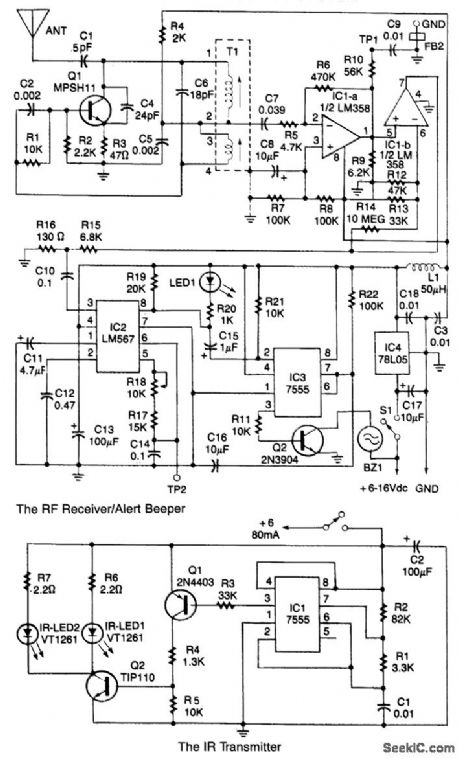

This system contains an IR transmitter, an IR receiver/RF transmitter, and an RF receiver/alert beeper. Two IR LEDs in the transmitter transmit a pulsed beam of invisible infrared light to the receiver, which contains an IR phototransistor. The phototransistor detects and amplifies the pulse-modulated IR beam. If the receiver section senses that the IR beam is momentarily interrupted by an object blocking the beam's path, it triggers the transmitter, which outputs a 49.890-MHz carrier that is amplitude-modulated by a 490-Hz tone.
Upon receiving the 490-Hz amplitude-modulated carrier, the RF receiver/beeper unit sounds an alarm that alerts the user to the intrusion. The system is not limited to just one RF transmitter. A single RF receiver/beeper can be used to monitor any number of RF transmitters (or locations). However, the receiver/beeper unit cannot discriminate between different transmitter sites in multiple-transmitter systems. (View)
View full Circuit Diagram | Comments | Reading(2075)
3_digit_ISUP2_SUP_L_A_D_converter_with_LCD
Published:2009/7/20 4:45:00 Author:Jessie

3-digit I2 L A/D converter with LCD (courtesy Analog Devices, Inc.). (View)
View full Circuit Diagram | Comments | Reading(1128)
The frequency spectrum therapeutic apparatus
Published:2011/7/21 20:11:00 Author:qqtang | Keyword: frequency spectrum, therapeutic apparatus

The working principle of the circuit
This frequency spectrum therapeutic apparatus consists of the power supply circuit, control circuit and frequency spectrum generator, see as figure 9-28.
The power supply circuit consists of the resistor R1-R5, switch S1-S3, dual-way trigger diode V, thyristor VT, capacitors C1 and C2, etc. The frequency spectrum generator consists of the voltmeter PV, rectifier VD1-VD4 and frequency spectrum heater EH. (View)
View full Circuit Diagram | Comments | Reading(486)
Complete_cassette_record_playback_circuitry_for_low_cost_devices_using_an_ECG1093_14_pin_DIP_with_tab
Published:2009/7/20 4:45:00 Author:Jessie

Complete cassette record/playback circuitry for low-cost devices using an ECG1093 14-pin DIP with tab. Typical power output is 1 watt. No signal current drain is 12 mA (courtesy GTE Sylvania Incorporated). (View)
View full Circuit Diagram | Comments | Reading(633)
| Pages:885/2234 At 20881882883884885886887888889890891892893894895896897898899900Under 20 |
Circuit Categories
power supply circuit
Amplifier Circuit
Basic Circuit
LED and Light Circuit
Sensor Circuit
Signal Processing
Electrical Equipment Circuit
Control Circuit
Remote Control Circuit
A/D-D/A Converter Circuit
Audio Circuit
Measuring and Test Circuit
Communication Circuit
Computer-Related Circuit
555 Circuit
Automotive Circuit
Repairing Circuit