
Circuit Diagram
Index 921
Step_down_switching_regulator_using_an_SH1605
Published:2009/7/20 21:04:00 Author:Jessie
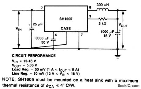
Step-down switching regulator using an SH1605. Output voltage is +5 volts. Available current is between 1 and 5 amperes. Input voltage is 12 to 18 volts. Line regulation is 2% with load regulation at 2%. Maximum ripple is 0.1 volt peak to peak (courtesy Fairchild Semiconductor). (View)
View full Circuit Diagram | Comments | Reading(558)
AUDIO_FADER
Published:2009/7/8 23:55:00 Author:May

In this circuit, Q1 is a simple amplifier that has its gain controlled by a variable emitter resistance supplied by FET Q2. In the up position of S1, C3 discharges through R5 and the gain of Q1 decreases because Q2 is driven toward cut-off. In the down position, Q2 conducts more, depending on the setting of R6, which causes a gain increase. By varying R5 or C3, various fade rates can be obtained. (View)
View full Circuit Diagram | Comments | Reading(1472)
STABILIZED_HORIZONTAL_OSCILLATOR
Published:2009/7/20 21:04:00 Author:Jessie

Sine-wave stabilization or ringing coil pulls Synchroguide horizontal oscillator frequency back to correct value when lube or other components drift in value.-W. E. Babcock, Unusual Tube Effects Cause Circuit Troubles, Electronics, 31:37, p 90-93. (View)
View full Circuit Diagram | Comments | Reading(939)
ARTIFICIAL_LARYNX
Published:2009/7/20 21:04:00 Author:Jessie

Output is negative pulse whose repetition frequency is varied from 100 to 200 cps by rheostat to change pitch of voice while speaking. Modified telephone receiver serves as vibrator that is pressed against throat to transform generated vibrations into speech sounds by normalmal use of throat cavity, tongue, mouth, teeth, and lips. With practice, users can achieve sentence intelligibility above 97%.-Circuit Substitutes as Larynx, Electronics, 32:27, p 60-63. (View)
View full Circuit Diagram | Comments | Reading(1397)
GASFET_FREQUENCY_DOUBLER
Published:2009/7/8 23:53:00 Author:May


This circuit will produce over + 10 dBm in the 1 800-3000-MHz range. Drive power is 7 dBm in the 900-to-1500-MHz range. The PC board is G-10 Epoxy doublesided. Artwork is shown above, as well as parts placement connectors suitable for these frequencies (such as SMA) should be used. A negative bias supply of 0 to 3 V is required. (View)
View full Circuit Diagram | Comments | Reading(630)
9_V_FROM_12_V
Published:2009/7/8 23:51:00 Author:May

Developed for economical operation of 9-V portable radio from 12-V storage battery of car-Circuits' 73 Magazine,Marche 1975.p 136 (View)
View full Circuit Diagram | Comments | Reading(517)
JFET_SERIES_PASS
Published:2009/7/8 23:50:00 Author:May

Use of JFET as series-pass element for LM3046 voltage regulator IC minimlzes battery drain In microprocessor systemapplications Pass element needs no preregu-lation because drive comes from reguiated output Gate source is isolated from line by drainand thus provides excellent line regulation.-J.Maxwell、Voltage Regulator Bridges Gap Between IC's and Zeners‘EDNMagazine.Sept 5、1977、p 178-179 (View)
View full Circuit Diagram | Comments | Reading(1040)
Programmable_power_supply_with_±100_volt_and_±50_volt_output
Published:2009/7/20 21:03:00 Author:Jessie
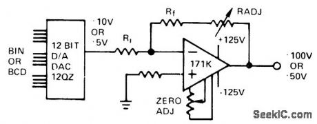
Programmable power supply with ±100-volt and ±50-volt output (courtesy Analog Devices, Inc.). (View)
View full Circuit Diagram | Comments | Reading(505)
SONIC_DEFENDER
Published:2009/7/8 23:49:00 Author:May


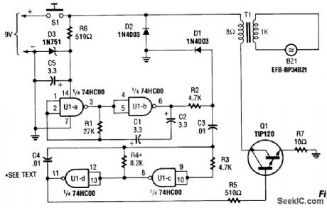
This oscillator-driver produces a deafening sound of about 3 kHz, modulated with a 10-Hz arble.BZ1 is a Matsushita EFB-RP34BZ. U1A and B generate the 10-Hz waveform that modulates the 3-kHz tone that is generated by U1C and D.Q1 drives the transducer through a 8-Ω:1-KΩ transformer. R4 might require slight changes ( ±1 kΩ) to optimize sound intensity.Warning: Could cause hearing loss if improperly used. (View)
View full Circuit Diagram | Comments | Reading(3519)
L_I_N_E_A_R_TRANSISTORIZED_HORIZONTAL_SWEEP
Published:2009/7/20 21:03:00 Author:Jessie

Placing transformer in yoke circuit provides better thon 0.5% linearity for deflecting 16.inch crt having 52° defection angle and 15-kv accelercation voltage. Line rate is 28.35 kc with 945 lines; Supply voltage determines width or amplitude of sweep. C can be increased to get 525-line rate.-J. W. Greininger, Improving Lineority in Transistorized Horizontal Sweeps, EEE, 12:9, p 61-62. (View)
View full Circuit Diagram | Comments | Reading(721)
HUM_FREE_TUNER_SUPPLY
Published:2009/7/8 23:49:00 Author:May

Permits operation of high-quality FM tuner from amplifier supply without having hum due to positive feedback through shared ground connection.Circuit provides up to 90 mA at 12 V from any supply ranging from 24 to 34 V. Low output impedance eliminates all likely sources of feed-back and suppresses ripple. Circuit requires careful initial adiustment to limit current sunk by 741C opamp to Iess than 15 mA; coarse adjustment is made by varying number of 47-ohm resistors in parallel serving as BD136 omitter re-sistor, and fine adjustment by changing R2.-G.Hibbert, Avoiding Power Supply Hum, Wireless Wolld, Oct. 1973, p 515. (View)
View full Circuit Diagram | Comments | Reading(535)
_10_V_AT_1_A
Published:2009/7/8 23:48:00 Author:May

Combination of LM195 power transistor IC and standard LM104 regulator gives negative output voltage with full overload protection and better than 2-mV load regula tion Input voltage must be only 2 V greater than output voltage,-″Linear Applications,Voi,2 National Semico"ductor、Santa Clara、CA'1976、AN-110,p4-5 (View)
View full Circuit Diagram | Comments | Reading(613)
48_V_FROM_80_V
Published:2009/7/8 23:47:00 Author:May
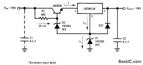
Level-shifting transistorzener combination R1-D2 is used with zener D1 to keap voltage across LM340-24 regulator below maximum ratedvalue Addition of zenershas drawback of inoreasing output noise to about 2 mV P-P. Load regulation is 60 mV for pulsed load change from 5 mA to 1 A. Line reg-ulation is 0.01%/V of input voltage change for 500-mA load.- Linear Applications, Vol. 2, National Semiconductor, Santa Clara, CA, 1976, AN-103, p 10-11. (View)
View full Circuit Diagram | Comments | Reading(2012)
10_volt_reference_from_a_12_volt_suppy
Published:2009/7/20 20:58:00 Author:Jessie
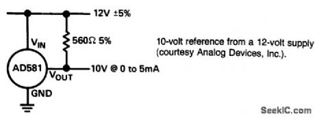
10-volt reference from a 12-volt suppy(courtesy Analog Devices,Inc.). (View)
View full Circuit Diagram | Comments | Reading(507)
AUDIO_FREQUENCY_DOUBLER
Published:2009/7/8 23:44:00 Author:May
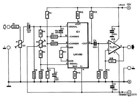
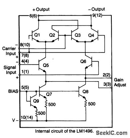
Often the frequency of a signal must be dou-bled: modulator/demodulator chip LM1496 is an ideal basis for this.
From trigonometry it is well known that:
2sitvrcosx= sin2x
and∶
sin2=1-xcos2x.
These equations indicate that the product of two pure sinusoidal signals of the same frequency is one signal of double that frequency. The purity of the original signals is important: composite signals would give rise to all sorts of undesired products.
The LM1496 can only process signals that are not greater than 25 mV: above that level, serious distortion will occur. The design is therefore pro-vided with a potential divider at its input. This addi-tion makes it possible, for instance, to arrange for a 500-mV input signal to result in a signal of only 25 mV at the input of the LM1496.
To provide a sufficiently high output signal, the output of IC1 is magnified by op amp IC2, which is connected as a noninverting amplifier. Because the output of IC1 contains a dc component of about 8 V, the coupling between the two stages must be via a capacitor, C4.
With values of R15 and R16 as shown, IC2 gives an amplification of 16 (24 dB). The overall amplifica-tion of the circuit depends on the level of the input signal: with an input of 1.2 V, the amplification is unity; when the input drops to 0.1 V, the amplification is just 0.1. The value of the input resistors has been fixed at 6800: this value gives a reasonable compromise between the requirements for a high input impedance and a low noise level.
To ensure good suppression of the input signal at the output, the voltages at pin 1 and pin 4 of IC1 must be absolutely identical to P4. It is possible, with the aid of a spectrum analyzer, to suppress the fundamental (input) frequency by 60 to 70 dB.
The output signal at pin 12 is distorted easily, because the IC is not really designed for this kind of operation. The distortion depends on the level of the input signal. At a frequency of 1 kHz and an input level of 100 mV, the distortion is about 0.6%; when the input level is raised to 500 mV, the distortion increases to 2.3%, and when the input level is 1 V, the distortion is 6%. The signal-to-noise ratio under these conditions varies between 60 and 80 dB.
The circuit draws a current of 10 mA from the positive supply line and 5 mA from the negative line.The phase shift between the input and output signals is about 45° (output lags). Finally, although the nor-mal output is taken from pin 12, a similar output that is shifted by 180° (with respect to that at pin 12), is available at pin 6. (View)
View full Circuit Diagram | Comments | Reading(1662)
15__20__25__35__50__60_watt_AF_power_amplifier_with_DC_coupled_output
Published:2009/7/20 20:58:00 Author:Jessie
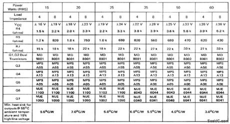
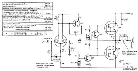
15-/20-/25-/35-/50-/60-watt AF power amplifier with DC-coupled output (courtesy Motorola Semiconductor Products Inc.). (View)
View full Circuit Diagram | Comments | Reading(1642)
1_TO_30_MHz_ANTENNA_TUNER
Published:2009/7/8 23:39:00 Author:May
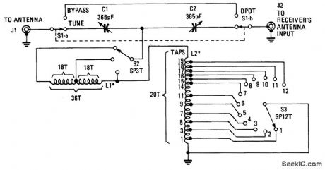
This tuner will match a random length wire antenna to a receiver or low-power transmitter (≤25 W) for optimum signal transfer. (View)
View full Circuit Diagram | Comments | Reading(2648)
+12_V_SERIES_EMITTER_FOLLOWER
Published:2009/7/8 23:38:00 Author:May

Baseemitter voltageis more orless constant withoutuse offeedback because baseis held at constant voltage by zener diode Ripple at base is reduced by RC filter.-H,Olson Power-Supply Servicing Ham Radio, Nov 1976、p44-50 (View)
View full Circuit Diagram | Comments | Reading(828)
PLETHYSMOGRAPH
Published:2009/7/20 20:57:00 Author:Jessie

Transistorized unit measures change in impedance of living tissue resulting from nonrythmic fluctuations of blood content Changes of 0.1% in total tissue impedance are detected by resistance bridge and phase-sensitive detector that scans bridge unbalance.-S. Bagno and F. M.Liebman, Impedance Measurements of Living Tissue, Electronics, 32:15, p 62-63. (View)
View full Circuit Diagram | Comments | Reading(2377)
SSB_GENERATORS
Published:2009/7/8 23:37:00 Author:May

These two circuits are SSB generators. One uses a crystal filter by KVG Electronics at 9 MHz, theother uses a 455-kHz mechanical filter. By feeding the outputs into a mixer, the frequency of the SSBgenerator can be converted to other frequencies.Keep signal levels low enough so that distortion does notoccur. (View)
View full Circuit Diagram | Comments | Reading(929)
| Pages:921/2234 At 20921922923924925926927928929930931932933934935936937938939940Under 20 |
Circuit Categories
power supply circuit
Amplifier Circuit
Basic Circuit
LED and Light Circuit
Sensor Circuit
Signal Processing
Electrical Equipment Circuit
Control Circuit
Remote Control Circuit
A/D-D/A Converter Circuit
Audio Circuit
Measuring and Test Circuit
Communication Circuit
Computer-Related Circuit
555 Circuit
Automotive Circuit
Repairing Circuit