
Circuit Diagram
Index 935
DOLBY_B_C_NOISE_REDUCTION_SYSTEM
Published:2009/7/8 22:03:00 Author:May

View full Circuit Diagram | Comments | Reading(565)
ANALOG_MULTIPLEXER_WITH_BUFFERED_INPUT_AND_OUTPUT
Published:2009/7/8 22:01:00 Author:May

This circuit is used for analog signal selection or time division multiplexing. As shown, the feedback signal places the selected amplifier channel in a voltage follower (noninverting unity gain) configuration, and provides very high input impedance and low output impedance. The single package replaces four input buffer amplifiers, four analog switches with decoding, and one output buffer amplifier. For low-level input signals, gain can be added to one or more channels by connecting the (-) inputs to a voltage divider between output and ground. The bandwidth is approximately 8 MHz, and the output will slew from one level to another at about 15.0 V per μs.
Expansion to multiplex 5 to 12 channels can be accomplished by connecting the compensation pins of two or three devices together, and using the output of only one of the devices. The enable input on the unselected devices must be low.
Expansion to 16 or more channels is accomplished easily by connecting outputs of four 4-channel multiplexers to the inputs of another 4-channel multiplexer. Differential signals can be handed by two identical multiplexers addressed in parallel. Inverting amplifier configurations can also be used, but the feedback resistors might cause crosstalk from the output to unselected inputs.
(View)
View full Circuit Diagram | Comments | Reading(1783)
KA2312 (toy) wireless remote control launch control regulation circuit
Published:2011/8/2 4:02:00 Author:TaoXi | Keyword: toy, wireless, remote control, launch, control, regulation circuit
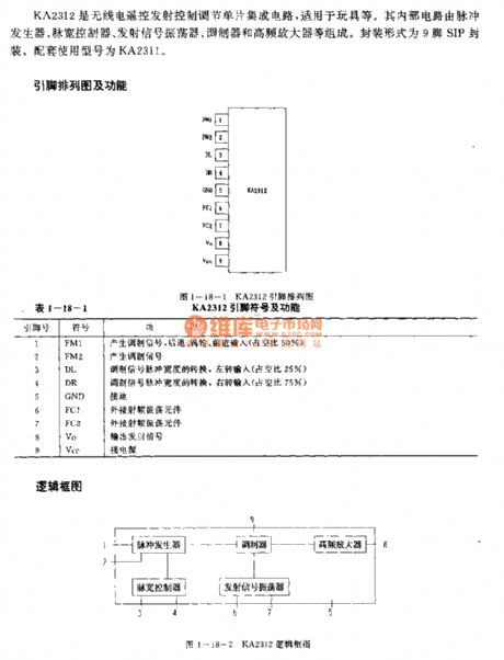
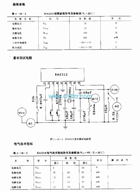
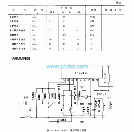
The KA2312 is designed as the wireless remote control launch control regulation circuit that can be used in the toy application. The internal circuit is composed of the pulse generator, the pulse width controller, the transmitting signal oscillator,the modulator, the high frequency amplifier and the automatic power switch. This device is in the 9-pin SIP package. The matching model is KA2311.
(View)
View full Circuit Diagram | Comments | Reading(1678)
VHF_TONE_TRANSMITTER
Published:2009/7/8 22:00:00 Author:May

The range of this transmitter is about 50 feet with a short whip antenna. The tone generator, is made up of a unijunction transistor, Q1, and R1, R2, R3, and C2. Transistor Q1 pulses on and off at a rate determined by the time constant of R1 and R2, together with the capacitance of C2 and the BI-emitter junction of Q1. Trimmer potentiometer R2 determines the frequency of the tone generated and allows a range of approximately 100 Hz to over 5 kHz.Transistor Q2 is the rf oscillator. Its frequency is set by tuned circuits consisting of L1, C5, C6, and the interelectrode capacitance of Q2. The values shown will give a tuning range of about 55 to 108 MHz. Capacitor C6 provides positive feedback from the emitter to the collector of Q2, for oscillation. The audio tone generated by Q1 is applied to the base of Q2, causing the collector current to vary at the frequency of the tone, yielding an amplitude-modulated (AM) signal. This, in turn, varies Q2's collector-to-emitter capacitance, which makes up part of the tuned circuit, and causes the output frequency to vary similarly, producing a frequency-modulated (FM) signal, as well. The rf signal is coupled to the antenna through capacitor C7.Coil L1 consists of five turns of #18 bare wire, close-wound on a piece of 1/4-inch wooden dowel. The length of the winding is about 1/4 inch. One end of capacitor C7 is soldered to the coil, one turn away from the 9-V supply end, and the other capacitor end is connected to the antenna. To adjust the vertical height and linearity of a TV set, place the tone transmitter near the set and use R2 to select the number of horizontal bars to be displayed. Once the picture is steady and the bars are sharp, adjust the set's vertical controls, so that all the bars are of the same height and are evenly spaced.The fact that both AM and FM signals are generated makes it possible to use this circuit to check almost any receiver within the transmitter's frequency range. A TV set's sound section (discriminator) will reject the AM portion of the signal, but its video section will respond to it. Similarly, the TV sound section and FM receivers will respond to the FM signal produced. (View)
View full Circuit Diagram | Comments | Reading(634)
THREE_CHANNEL_MULTIPLEXER_WITH_SAMPLE_AND_HOLD
Published:2009/7/8 22:00:00 Author:May

View full Circuit Diagram | Comments | Reading(551)
AM_detector_AGC_amplifier_and_SSB_demodulator
Published:2009/7/23 21:39:00 Author:Jessie

The SL623 shown provides all three functions on a single chip, and is designed specifically for used in SSB/AM receivers (in conjunction with SL610/SL611/SL612 RF and IF amplifiers). With the values shown, typical characteristics are: SSB audio output 30 mV (rms), AM audio output 55 mV (rms), AGC range 6 dB (change in input level to increase AGC output voltage from 2.0 to 4.6 V), with an input impedance of 800Ω at pins 6/9, maximum frequency 30 MHz, and an AM carrier level down to 100 mV. (View)
View full Circuit Diagram | Comments | Reading(1625)
TOY_TRAIN_CONTROL
Published:2009/7/23 21:44:00 Author:Jessie
With L1-C1 tuned to one of five r-f channels (100, 140, 180, 220 and 255 kc), pair of scr's drives train either forward or in reverse, depending on polarity of r-f signal pulse applied to rails by control station. Five-channel transmitter permits simultaneous control of five different trains, each having receiver tuned to different frequencies. Scr characteristics eliminate jackrabbit starts.-S. B, Gray, Appliances and Housewares, Electronics, 36:20, p 46-49. (View)
View full Circuit Diagram | Comments | Reading(614)
AM_IF_and_detector
Published:2009/7/23 21:44:00 Author:Jessie

The SL6701 shown is a single- or double-conversion IF amplifier anddetector for AM-radio applications. Normally,the SL6701 is fed with a first IFsignal of 10.7 or 21.4 MHz There is amixerforconversion to the firstorsecond IF,a detector, and an AGC generator with optional delayed output. (View)
View full Circuit Diagram | Comments | Reading(847)
Portable_receiver
Published:2009/7/23 21:52:00 Author:Jessie
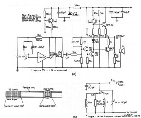
Figure 2-16A shows the ZN414Z (Fig. 2-14A) combined with extemal components to form a portable receiver (known as a Triffid receiver). Figure 2-16B shows the coil-winding details and waveband-selection circuits. (View)
View full Circuit Diagram | Comments | Reading(1140)
GM3043 (TV and video tape recorder) infrared remote control launch circuit
Published:2011/8/1 9:01:00 Author:TaoXi | Keyword: TV, video tape recorder, infrared, remote control, launch circuit
The GM3043 has the same functions and pin arrangement with the uPD1943G, so they can exchange directly. The technical characteristics, absolute maximum ratings, main electrical specifications, logic diagram and typical application circuits of the GM3043 can reference the uPD1943G's. (View)
View full Circuit Diagram | Comments | Reading(747)
On_leakage_current_tests
Published:2009/7/23 21:52:00 Author:Jessie

Figure 2-K shows a basic test circuit for measuring on-leakage-current I D(ON) for the MAX326/27. Figure 2-L shows how I D(ON) changes with temperature. (View)
View full Circuit Diagram | Comments | Reading(820)
Fast_12_bit_A_D_converter
Published:2009/7/23 21:52:00 Author:Jessie
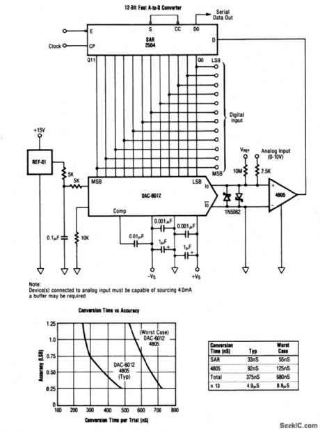
This circuit shows a DAC and comparator that is used with an SAR to form a 12-bit A/D converter. The analog input (0 to +10 V) is applied at the 4805 comparator noninverting input. Both parallel and serial digital outputs are available VREF can be trimmed for zero. Full-scale is trimmed by adjustment of the REF-01. (View)
View full Circuit Diagram | Comments | Reading(1415)
CONTACT_TESTER
Published:2009/7/23 21:53:00 Author:Jessie

Determines whether contacts have maintained their normally open or closed conditions during shock and vibration testing. Dual circuit monitors both types of contact.-F. W. Kear, Contact Monitoring for Vibration Tests, Electronics, 33:15, p 78-79. (View)
View full Circuit Diagram | Comments | Reading(634)
YN5101 (electric fan) infrared remote control coding circuit
Published:2011/8/1 9:06:00 Author:TaoXi | Keyword: electric fan, infrared, remote control, coding circuit
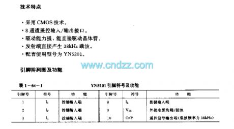
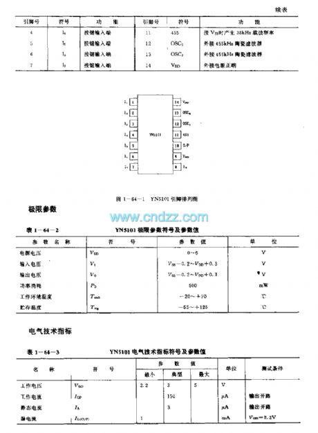

Features
It uses the CMOS technology.The 8-channel remote control output/input interface.The drive capability is strong, it can drive the transistor directly.The transmitter port produces the 38kHz carrier wave directly.The matching model is YN5201.
(View)
View full Circuit Diagram | Comments | Reading(2391)
LOW_NOISE_UHF_TV_TUNER
Published:2009/7/23 21:53:00 Author:Jessie
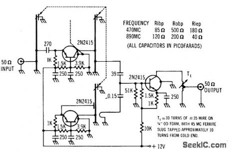
Input is tunable from 470 to 890 Mc, and output is 45 Mc.Gain is 3 to 9 db over uhf band, with typical noise figure of 7 to 9 db.-Texas Instruments Inc., Solid-State Communications, McGraw-Hill, N.Y., 1966, p 299. (View)
View full Circuit Diagram | Comments | Reading(721)
Konka R878 mobile phone cable connection figure
Published:2011/8/3 1:21:00 Author:Ecco | Keyword: Konka , mobile phone , cable connection

View full Circuit Diagram | Comments | Reading(588)
Fast_charge_controllers_for_NiCcld_NiMH
Published:2009/7/27 0:25:00 Author:Jessie
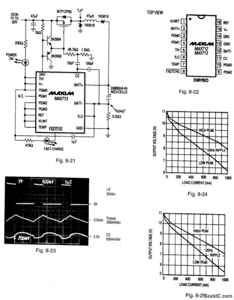
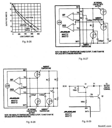
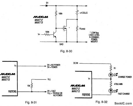
Figure 8-21 shows a MAX713 connected to provide a fast charge for two cells at 1 A. Higher charge currented and greater number of cells can be accommodated by changing RSENSE and the PGMO-PCM3 connections (as described in the date sheet).Figure 8-22 shows the pin connections and Fig. 8-23 shows the circuit waveforms. Notice that the circuit of Fig. 8-21 cannot service a loud while charging. The Fig. 8-21 circuit is usually used with an ac-to-dc wall cube (transformer,bridge rectifier, and capactior in a plug-in package).Figures 8-24.8-25,and 8-26 show the characteristics of three consumer-product wall cubes. when selecting a wall cube, be sure that the lowest dip in the wall-cube voltage. Figure 8-27 shows the connections for controlling charge cutoff with negative-temperature-coefficient (NTC) thermistors. Use the same model of thermistor for T1 and T2 so that both have the same nominal resistance. The voltage at TEMP is 1 V (referred to batt-) when the battery is at ambient temperature.some battery pavks might come with a temperature-detecting thermistor connected to the negative terminal of the battery pack. In this case, use the connections shown in Fig. 8-28. T2 and T3 can be replaced with standard resistors if absolute temperature cutoff is acceptable.The absolute maximum voltage rating for the BATT+ input voltage must be limited by external circuits when DC IN is not applied, as shown in Fig. 8:29. Rsense causes a small efficiency loss during battery use. The efficiency loss is significant only if Rsense is much greater than the internal resistance of the battery pack. The circuit of Fig. 8-30 can be used to shunt Rsense whenever power is removed from the charger. Figure 8-31 shows a circuit used to indicate charger status, with logic-level outputs. Figure 8-32 shows an LED drive circuit that indicates charger status. MAXIM NEW RELEASES DATA BOOK, 1994, P. 4-60, 4-61, 4-63, 4-64. (View)
View full Circuit Diagram | Comments | Reading(726)
Konka R878 mobile phone cable connection schematic diagram
Published:2011/8/3 1:24:00 Author:Ecco | Keyword: Konka , mobile phone , cable connection

View full Circuit Diagram | Comments | Reading(1182)
Digital_tare_compensation
Published:2009/7/25 5:41:00 Author:Jessie
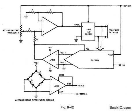
Figure 9-42 shows a DAC0830 and an ADC0801 connected to provide digital tare compensation. Such a function is used in a weighing system in which the weight of the scale platform, and possibly a container, is subtracted automatically from the total weight being measured. This expands the range of weight that can be measured by preventing a premature full-scale reading and allows an automatic indication of the actual unknown quantity. The DAC is initially given a zero code, and the system input is set to a reference quantity. A conversion of the input is performed, then the corresponding code is applied to the DAC. The DAC output is then equal to and of opposite polarity to the input voltage. This forces the amplifier output, and the ADC input, to zero. (In this case, an 8-bit ADC is used.) The DAC output is held constant so that any subsequent ADC conversion will yield a value relative in magnitude to the initial reference quantity. To ensure that the output code from the ADC generates the correct DAC output voltage, the two devices should be driven from the same reference voltage. For differential input signals, an instrumentation amplifier (such as an LM363) can be used. The output reference pin of the LM363 can be driven directly by the DAC, as shown. This will offset the ADC input. NATIONAL SEMICONDUCTOR, APPLICATION NOTE 271, 1994, P. 670. (View)
View full Circuit Diagram | Comments | Reading(1697)
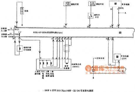
BMW8 Series of EGS 35pin (4HP-22/24) transmission circuit diagram 1
Published:2011/8/3 2:20:00 Author:Ecco | Keyword: BMW8 Series , EGS , 35pin transmission
View full Circuit Diagram | Comments | Reading(488)
| Pages:935/2234 At 20921922923924925926927928929930931932933934935936937938939940Under 20 |
Circuit Categories
power supply circuit
Amplifier Circuit
Basic Circuit
LED and Light Circuit
Sensor Circuit
Signal Processing
Electrical Equipment Circuit
Control Circuit
Remote Control Circuit
A/D-D/A Converter Circuit
Audio Circuit
Measuring and Test Circuit
Communication Circuit
Computer-Related Circuit
555 Circuit
Automotive Circuit
Repairing Circuit