
Circuit Diagram
Index 928
Precision_AGC_circuit_using_an_AD531_multiptter_divider_and_an_AD741_op_amp
Published:2009/7/21 2:52:00 Author:Jessie
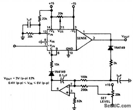
Precision AGC circuit using an AD531 multiptter/divider and an AD741 op amp. The circuit works by rectifying a signal and comparing it with thevoltage at the set level pot. The comparator output is then applied as a control signal to the AD531. The circuit can regulate VOUT to 3 volts peak to peak for inputs from 0.4 volt peak to peak to 6.0 volts peak to peak from 30 hertz to 400 kilohertz (courtesy Analog Devices, Inc.). (View)
View full Circuit Diagram | Comments | Reading(1085)
1_watt_inverting_power_amplifier_using_an_MC1554
Published:2009/7/21 2:53:00 Author:Jessie
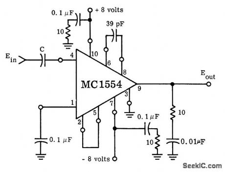
1-watt inverting power amplifier using an MC1554. As shown the voltage gain is 35. An external heat sink is required for dissipation greater than 350 mW (courtesy Motorola Semiconductor Products Inc.). (View)
View full Circuit Diagram | Comments | Reading(562)
Pulse_power_amplifier_using_an_MC1554
Published:2009/7/21 2:54:00 Author:Jessie

Pulse power amplifier using an MC1554. As shown voltage gain is 18. Peak power of 3 watts is possible (courtesy Motorola Semiconductor Products Inc.). (View)
View full Circuit Diagram | Comments | Reading(518)
STABLE_INDUCTIVE_TUNED_OSCILLATOR
Published:2009/7/21 2:56:00 Author:Jessie

In frequency-shift keying (FSK) applications, when modulating high data rates, coupling data to the varactor can pose a problem. A duplex filter is necessary to prevent RF loading or leaking of the oscillator tank while transferring the fast data edges to the varactor. These two constraints contradict one another-especially when the edge's rise time approaches that of the carrier frequency. If an RF choke or a large-value resistor is used to inject data to the varactor, then the edges of the data will be severely distorted by RC or inductive-capacitive (LC) time constants. The loss of these rise times can result in duty-cycle distortion as seen by the threshold level detector in the receiver. To improve upon the traditional VCO techniques, varying the inductor provides increased tuning sensitivity and better resonator Q. Inductive tuning uses the coupling or leakage inductance characteristics of a transformer. Thus, tuning capacitor C4 can be changed to a fixed, high-quality capacitor. Use of a negative -temperature -coefficient capacitor here can balance out the active device's capacitance variation with temperature. The tuning inductor (L1) is now a transformer. At about 48 MHz, it is a nine-turn, center-tapped coil of AWG28 wound on a 725-10 Micrometals core. Other transformers also can be implemented, depending on operating frequencies and performance requirements. The Q for this inductor is about 100, which is more than sufficient to isolate the active device to prevent its pulling the oscillator tank over the extended temperature range of -40 to 85℃. The inductance variation or stability with temperature is dependent on the core material of L1. (View)
View full Circuit Diagram | Comments | Reading(1001)
Multiple centralized control regulated power supply circuit diagram
Published:2011/8/2 1:27:00 Author:Rebekka | Keyword: Multiple centralized control, regulated power supply
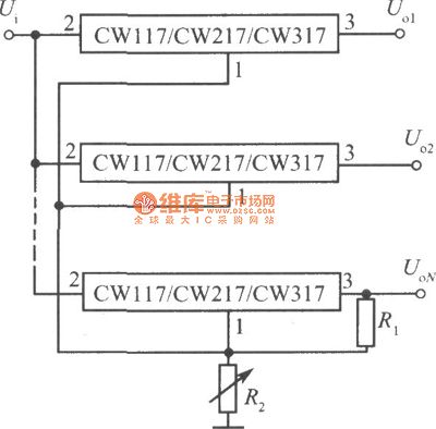
Multiple centralized control regulated power supply circuit composed of multiple three-terminal adjustable integrated voltage regulators is shown as above.
The figure shows the integrated centralized control of multiple power supply composed of a number of three-terminal adjustable regulators. All the input terminals of the integrated voltage regulators is connected togetherand they share the same power supply. All the adjustment terminals are connected together. The resistance Rl and R2 control the output voltage. For keeping the output voltage deviation of each integrated regulator is less than 100mV, the load current of each printed circuit board should be less than 10mA. Otherwise, the output voltage deviation will be significantly increased. (View)
View full Circuit Diagram | Comments | Reading(582)
BIAS_SUPPLY_FOR_MICROWAVE_PREAMPS
Published:2009/7/8 23:07:00 Author:May


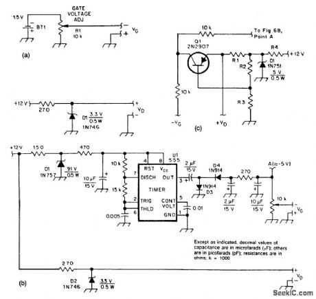


These two circuits provide bias for the microwave preamps shown in this text. The circuit in Fig.51-5(a) is a simple passive supply. Figures 51-5(b) and 51-5(c) are active supplies, with U1 generating a negative supply and Q1 setting the drain voltage and current, independent of GASFET haracteristics.
(View)
View full Circuit Diagram | Comments | Reading(524)
TREMOLO_1
Published:2009/7/8 23:07:00 Author:May

A phase shift oscillator using the LM324 operates at an adjustable rate, 5-10 Hz, set by the speed pot. A potion of the oscillator output is taken from the depth pot and used to modulate the on resistance of two 1N914 diodes operating as voltage controlled attenuators. Care must be taken to restrict the incoming signal level to less than 0.6 V pk-pk, or undesirable clipping will occur. (View)
View full Circuit Diagram | Comments | Reading(587)
Inexpensive_high_performance_gain_control_circuit
Published:2009/7/21 2:56:00 Author:Jessie
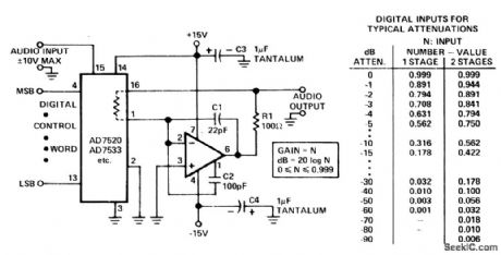
Inexpensive high-performance gain control circuit (courtesy Analog Devices, Inc.). (View)
View full Circuit Diagram | Comments | Reading(547)
Two_quadrant_multiplier_using_a_Datel_DAC_IC10BC_D_A_convener
Published:2009/7/21 2:57:00 Author:Jessie

Two-quadrant multiplier using a Datel DAC-IC10BC D/A convener. The DAC-IC10BC chip is a 16-pin DIP. VIN is unipolar and the digital input is bipolar with offset binary coding. VOUT varies over the bipolar range of ±5 volts. It is recommended that full scale IREF be set to 2.0 mA; the output is then monotonic as the reference current varies over 0.5 mA to 2.0 mA (courtesy Datel Systems, Inc.). (View)
View full Circuit Diagram | Comments | Reading(1867)
LOW_NOISE_OSCILLATOR
Published:2009/7/21 2:57:00 Author:Jessie

This oscillator is suitable for low-noise applications. L is wound on a 6-mm form, and C is 15 to 220 pF. The frequency range is 20 to 80 MHz. The output is 0 dBm into 50 Ω. For use of the circuit as a crystal-controlled oscillator, a crystal can be inserted as shown. (View)
View full Circuit Diagram | Comments | Reading(714)
Vector_magnitude_function_from_the_4301_multifunction_chip
Published:2009/7/21 2:57:00 Author:Jessie

Vector magnitude function from the 4301 multifunction chip (courtesy Burr-Brown Research Corporation). (View)
View full Circuit Diagram | Comments | Reading(466)
TTL_RING_OSCILLATOR
Published:2009/7/21 2:58:00 Author:Jessie

A TTL ring-oscillator circuit uses an odd number of inverters in an astable configuration. (View)
View full Circuit Diagram | Comments | Reading(791)
Stable_instrument_amplifier_for_lab_equipment_and_panel_meters
Published:2009/7/21 2:59:00 Author:Jessie

Stable instrument amplifier for lab equipment and panel meters. The amplifier is noninverting and offers selectable gains from 1 to 1000 in decade steps. Input impedance is 10M (courtesy Analog Devices, Inc.). (View)
View full Circuit Diagram | Comments | Reading(533)
FRANKLIN_OSCILLATOR
Published:2009/7/21 2:59:00 Author:Jessie

Shown in tube form, this circuit shows the principle and the configuration of the Franklin oscillator.
The basic Franklin master oscillator, first described in 1930, uses very low-value capacitors, C1 and C2 (about 1 to 3 pF), imposing a very light load on the high-Q tuned circuit. Further advantages include the two-terminal inductance and the earthing of one end of the resonant circuit. This form of oscillator can be readily adapted for use with MOSFET devices. (View)
View full Circuit Diagram | Comments | Reading(2108)
0 to 20V 1A adjustable regulated power supply circuit diagram
Published:2011/5/10 2:30:00 Author:Rebekka | Keyword: adjustable regulated power supply

0 to 20V 1A adjustable regulated power supply circuit diagram composed of LM120-15 and zener diode LM741. (View)
View full Circuit Diagram | Comments | Reading(718)
OPAMP_DRIVES_POWER_DARLINGTONS
Published:2009/7/21 1:26:00 Author:Jessie
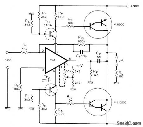
Differential outputs for Darlingtons are obtained by using power supply pins of 741 opamp. Tr1 and Tr2 can be any general-purpose transistors, and individual transistors can replace Darling-ton pairs. If circuit is used in servo system, add components shown in broken lines for zeroing of output offset. With values shown, 30 W can be delivered into 8 ohms from DC to 100 kHz at gain of 10 with less than 0.2% distortion.-K. Griffiths, Novel Power Amplifier, Wireless World, Dec. 1974, p 504. (View)
View full Circuit Diagram | Comments | Reading(2377)
Tracking integrated power supply circuit composed of two CW117 CW217 CW317
Published:2011/8/3 2:40:00 Author:Rebekka | Keyword: Tracking integrated power supply

View full Circuit Diagram | Comments | Reading(492)
44_VAC_DRIVE
Published:2009/7/21 1:27:00 Author:Jessie
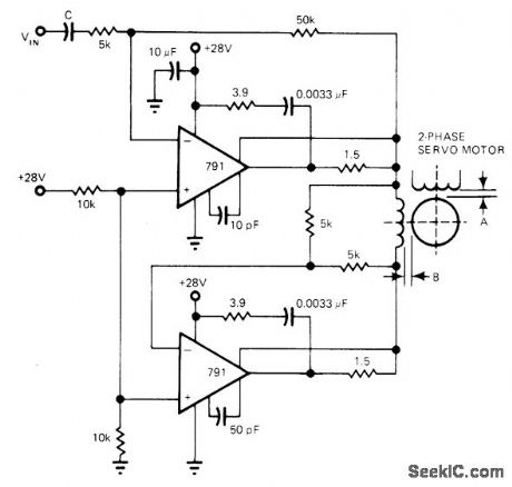
Uses two 791 power opamps, each rated for 10-W continuous dissipation, in AC bridge. Upper 791 has inverting gain of 10.Lower 791 inverts its output so 44 V P-P signal is applied across two-phase AC servomotor.-R. J. Apfel, Power Op Amps-Their Innovative Circuits and Packaging Provide Designers with More Options, EDN Magazine, Sept. 5, 1977, p 141-144. (View)
View full Circuit Diagram | Comments | Reading(604)
The morning and night light-operated switch circuit diagram with 10-10LX light intensity
Published:2011/8/3 2:42:00 Author:Rebekka | Keyword: morning and night , light-operated switch , 10-10LX light intensity
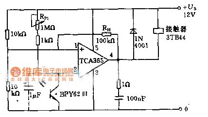
The power of 8.5KW load off can be controlled by using the input phototransistor BPY62 and power operational amplifier.The voltage divider composed of two 10KΩ resistors connects to the inverting input terminal of the voltage divider, so that the turnover voltage of the amplifiers is 1/2 US. Switch sensitivity can be adjusted in the range of 10 - 10 quadruplicate lx by using potentiometer. The output of the circuit is controlled by contactor coil. (View)
View full Circuit Diagram | Comments | Reading(1488)
Power_generation_circuit_using_n_AD7523_8_bit_multiplying_D_A_conveners
Published:2009/7/21 1:28:00 Author:Jessie


Power generation circuit using n AD7523 8-bit multiplying D/A conveners (courtesy Analog Devices, Inc.). (View)
View full Circuit Diagram | Comments | Reading(867)
| Pages:928/2234 At 20921922923924925926927928929930931932933934935936937938939940Under 20 |
Circuit Categories
power supply circuit
Amplifier Circuit
Basic Circuit
LED and Light Circuit
Sensor Circuit
Signal Processing
Electrical Equipment Circuit
Control Circuit
Remote Control Circuit
A/D-D/A Converter Circuit
Audio Circuit
Measuring and Test Circuit
Communication Circuit
Computer-Related Circuit
555 Circuit
Automotive Circuit
Repairing Circuit