
Circuit Diagram
Index 924
145_MHz_RF_oscillator_using_a_3N204_3N211_dual_gate_MOSFET
Published:2009/7/20 23:56:00 Author:Jessie
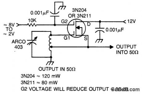
145 MHz RF oscillator using a 3N204/3N211 dual-gate MOSFET (courtesy Texas Instruments Incorporated). (View)
View full Circuit Diagram | Comments | Reading(2508)
100_KC_HYBRID_BALANCED_MODULATOR
Published:2009/7/21 0:09:00 Author:Jessie
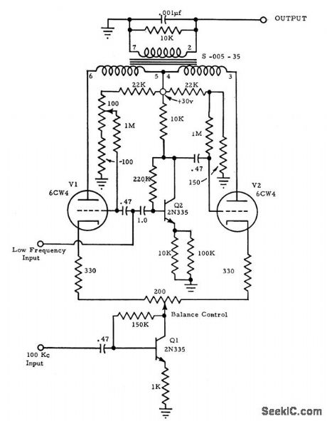
Circuit is essentially balanced bridge, with carrier injected by Q1. Balance is maintained by balance control and by bias adjustment on VI. Modulation is achieved by unbalancing bridge in accordance with low-frequency in.put signal, using phase inverter Q2 to make both tubes unbalance bridge in same direction.-J. Chirnitch, Hybrid Balanced Modulator for 100 Kc, EEE, 10:10, p 30. (View)
View full Circuit Diagram | Comments | Reading(1079)
TRANSFORMER_T_R_I_G_G_E_R_E_D_MAGNETRON_MODULATOR
Published:2009/7/21 0:10:00 Author:Jessie
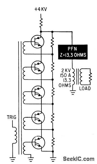
Success of circuit depends on availability of five pnpn transistors with breakover voltages of at least 800 v, in order to deliver 300-kw pulses to load through pulse-forming network PFN.-F. A. Gateka and M. L. Embree, Semiconductor Modulators for Modem Magnetrons, Electronics, 35:37, p 42-45. (View)
View full Circuit Diagram | Comments | Reading(599)
1296_MHz_RF_AMPLIFIER
Published:2009/7/9 1:16:00 Author:May
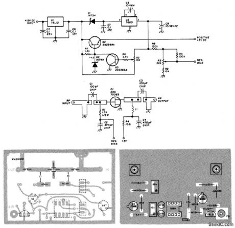
Using an NEC70083, this 1296-MHz amplifier delivers about 17-dB gain and around 1- to 1.5-dB noise. It is constructed on a G-10 epoxy fiberglass PC board. Use the layout shown because this is impor-tant for correct performance.The power supply/regulator delivers the regulated 3-Vdc for the drain circuit and U2 produces a nega-tive bias for the gate circuit. R5 sets the drain voltage to+3 V and R3 sets the gate bias. Typically, the drain current is about 10 mA. (View)
View full Circuit Diagram | Comments | Reading(1054)
DISCRETE_SEQUENCE_OSCILLATOR
Published:2009/7/9 1:15:00 Author:May

The swept-frequency oscillator offers an inexpensive source of discrete frequencies for use in testing digital circuits. In this configuration, the circuit generates an 80-second sequence of eight frequencies, dwelling for 10 seconds on each frequency. You can change the dwell time or the number of frequencies.Frequencies can range from 0.005 Hz to 1 MHz.
The programmable crystal oscillators, PXOs, IC2 and IC4 can each generate 57 frequencies in response to an 8-bit external code. IC2 contains a 1-MHz crystal and produces a 0.05-Hz output. IC4 contains a 600-kHz crystal; its output changes in response to the combined outputs of the 12-stage binary counter IC3 (Q1 and Q2) and the PXO IC2.
To generate more frequencies, you can use one or more of IC3's outputs, (Q3, Q4, Q5) to drive one or more of IC4's inputs (P4, P5, P6). Similarly, you can rewire IC2 or drive it with other logic to control the duration of each frequency. IC1, a monostable multivibrator, provides a system reset. It initiates the sequence shown, beginning at 60 Hz, in response to a positive pulse. (View)
View full Circuit Diagram | Comments | Reading(716)
RF_ATTENUATOR
Published:2009/7/8 23:29:00 Author:May
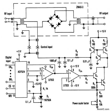
A balanced mixer is used as a control element in this circuit. An Analog Devices AD7524 D/A con-verter drives a voltage-controlled current source using two LF353s and several transistors to control the balanced mixer, a Mini Circuits Lab Z MAS-3
(View)
View full Circuit Diagram | Comments | Reading(1358)
ULTRASONIC_PEST_REPELLER
Published:2009/7/8 23:28:00 Author:May

This circuit is a 555 timer IC connected as a square-wave generator. Its base frequency is approximately 45 kHz, as determined by the values of R1, R2, and C1. The 45-kHz carrier is frequency modulated by a modified trapizoidal voltage waveform applied to pin 5 of the 555 timer. That modulating voltage is developed by a network consisting of C2, R3, and R4 connected across one leg of the bridge rectifier. The sweep is approximately 20 kHz on each side of the base frequency. The speaker is a 2-inch piezoelectric tweeter. (View)
View full Circuit Diagram | Comments | Reading(0)
2__37_V
Published:2009/7/8 23:27:00 Author:May

Simple circuit glves fine linear controlwith 10-turn pot over wide voltage range by first using 10K trimmer pot to divide 7-V reference down to 2 V.-G. Dressel, Regulator Circuit Provides Linear 2-37 V Adjustment Range, EDNMagazine, March 5, 1978, p 122. (View)
View full Circuit Diagram | Comments | Reading(912)
TURNTABLE_RUMBLE_FILTER
Published:2009/7/8 23:27:00 Author:May

Many record players unfortunately exhibit two undesired side effects: rumble (noise caused by the motor and the turntable) and other low-frequency spurious signals. The active high-pass Chebyshev filter presented here was designed to suppress those noises. The filter has a 0.1-dB ripple characteristic and a cut-off point of 18 Hz.
The choice of a Chebyshev filter might not seem optimum for audio purposes, but because of its 0.1-dB ripple in the pass band it behaves very much like a Butterworth type. Its advantage is that the response has steeper skirts (which are calculated curves). Frequencies below 10 Hz are attenuated by more than 35 dB. The phase behavior in the pass band shows a gradual shift so that its effect on the repro-duced sound is inaudible.
If the filter is used in a stereo installation, the characteristics of both filters must be identical or nearly so. Phase differences between channels can be heard-perhaps not so much at lower frequencies, but certainly in the midranges. To ensure identity and also to obtain the desired characteristics, capacitors C1 through C5 must be selected carefully. It does not matter much whether their value is 467 or 473 pF; this difference only causes a slight shift of the cut-off point. However, they must be identical within that 1% tolerance. For symmetry of channels, the capacitors can be paired and then used in either channel at the corresponding position.
The diagram shows theoretical values for the resistors: their practical values are given in the table.The prototype was constructed with 5% metal-film types from the E12 series and these were used with-out sorting. Their tolerance was perfectly acceptable in practice.
The current drawn by the circuit is purely that through the op amp and it amounts to about 4 mA. The high cut-off point is also determined by the op amp and it lies at about 3 MHz.
The only problem that cannot be foreseen is a possible coupling capacitor in the signal source. That component will be in series with C1 and this might adversely affect the frequency response. However, if its value is greater than 47 μF, it will have little if any effect; if it is below that value, it is best removed; C1 will assume its function. (View)
View full Circuit Diagram | Comments | Reading(2596)
±15V_AT_200_mA
Published:2009/7/8 23:26:00 Author:May

Two-opamp regulatorgives dual-polarity tracking outputs that can be balanced to within millivolts of each other or can be offset as required. Negative voltage is regulated, and positive output tracks negative. Article gives step-by-step design procedure based on use of pA741 or equivalent opamps. AC ripple is less than 2 mV P-P. Conventional full-wave bridge rectifier with capacitor-input filter can be used to provide rectuired unregulated 36 VDC for inputs.-C. Brogado, IC Op Amps Simplify Regulator Design, E.DNlEEEMagazine, Jan.15, 1972, p 30-34. (View)
View full Circuit Diagram | Comments | Reading(766)
1A_WITH_0005_VOLTAGE_ACCURACY
Published:2009/7/8 23:26:00 Author:May

Use of National LM120 negative regulator with LM108A low-drift opamp and 1N829 precision reference diode gives extremely tight regula-tion, very low temperature drift, and full over load protection. Bridge arrangement sets output voltage and holds reference diode current constant. FET is required because 4-mA maximum ground current of regulator exceeds output current rating of opamp. R1 and R2 should track to 1 PPM or less. R3 is chosen to set reference current at 7.5 mA. For output of 8 to 14 V, use LM120-5.0; for 15-17V, use LM120-12.-C. T. Nelson, Power Distribution and Regulation Can Be Simple, Cheap and Rugged, EDNMagazine, Feb. 20, 1973, p 52-58. (View)
View full Circuit Diagram | Comments | Reading(755)
_3V
Published:2009/7/8 23:25:00 Author:May
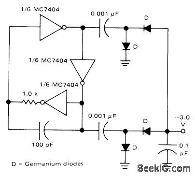
Circuit using three sections of Motorola MC7404 operates from +5 V supply and gen-erates -3 V at up to 100 μA, as one of supply voltages required by Motorola MCM6570 8192-bit character generator using 7 x 9 matrix.- A CRT Display System Using NMOS Memories, Motorola, Phoenix, AZ, 1975, AN.706A, p 5.|| (View)
View full Circuit Diagram | Comments | Reading(724)
DIODE_SENSOR_FOR_LASERS
Published:2009/7/8 23:25:00 Author:May


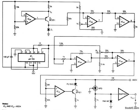
Laser-receiver circuits must bias their avalanche photo diodes (APD) to achieve optimal gain. Unfor-tunately, an APD's gain depends on the operating temperature. The circuit controls the operating voltage of an APD over a large temperature range to maintain the gain at the optimal value. The circuit uses D1 as a temperature sensor, thermally matched with the APD.A voltage regulator, IC1, supplies the necessary reference voltage to the circuit. IC2A and Q1 bias D1 at a constant current. IC2B, IC2C, IC3A/IC3B, and IC3C amplify D1's varying voltage and set Q2 to he optimal-gain corresponding value. Potentiometer RI controls the amplification over a range of 5 to 5. R2 controls the voltage level, which corresponds to the optimal gain of the APD at 22°C (the erature is specific to the type of APD). The circuit shown was tested with an RCA C 30954E APD. The tests cov-ered -40 to +70°C and used a semiconductor laser. The laser radiation was transmuted on the APD's active surface in the climatic room via fiberoptic cable. The gain varied by, at most, 10.2 dB over the entire temperature range. (View)
View full Circuit Diagram | Comments | Reading(1287)
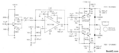
STEP_SERVO_CONTROL
Published:2009/7/21 1:16:00 Author:Jessie
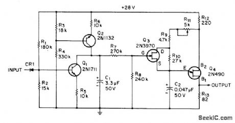
Variable UJT oscillator generates train of pulses under control of digital input logic levels, at 1000 pulses per second for logic 1 or 4400 pulses per second for logic 0, with smooth transitions between rates when logic changes, for driving stepping servomotor. Q1 and Q2 are constant-current sources. JFET Q3 acts as voltage-controlled variable resistor in parallel with R10, controlling pulse rate of UJT oscillator Q4.-C.R.Forbes.Step-Servo Motor Slew Generator. EEE Magazine.Oct.1970,p76-77. (View)
View full Circuit Diagram | Comments | Reading(662)
_5V_WITH_MC146OG
Published:2009/7/8 23:24:00 Author:May

Series power transistor and Motorola IC voltage regulator provide up to 100 mA. IC shown has been replaced by MC1469. Equivalents made by other manufac-turers can also be used.-H. Olson, Power-Sup-ply Servicing, Ham Radio, Nov. 1976, p 44-50. (View)
View full Circuit Diagram | Comments | Reading(696)
ULTRASONIC_RECEIVER
Published:2009/7/8 23:23:00 Author:May

The 4046 PPL is used as the heart of a tunable ultrasonic receiver that can be used to locate unheard ultrasonic sounds. The receiver might also be used, along with a simple ultrasonic generator, to send and receive Morse code. The incoming ultrasonic signal is picked up by piezo speaker SPKRl, and amplified by transistors Q1 and Q2. The output is fed to the phase comparator input of U1 at pin 14. The chip's interval VCO is tuned by turning potentiometer R9.If a 20-kHz signal is picked up by SPKR1 and the VCO is tuned to produce a 19-kHz signal the difference output at pin 2 will be 1 kHz. That 1-kHz signal is amplified by Q3 and coupled through T1 to a pair of headphones. If the received frequency increases to 22 kHz, a 3-kHz tone is heard in the headphones. With the values given in the parts list for C1, R1, and R9, the VCO can be tuned from 12 to well over 42 kHz, which should cover just about anything the piezo sensor can respond to. (View)
View full Circuit Diagram | Comments | Reading(0)
TWO_PHASE_SERVO_DRIVE
Published:2009/7/21 1:17:00 Author:Jessie
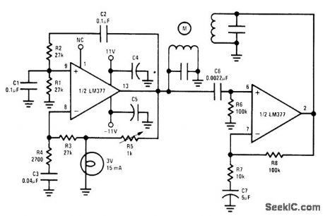
Both sections of National LM377 power amplifier are connected to provide up to 3 W per phase for driving small 60-Hz two-phase servomotor. Power is sufficient for phonograph turntable drive. Lamp is used in simple amplitude stabilization loop. Motor windings are 8 ohms, tuned to 60 Hz with shunt capacitors.- Audio Handbook, National Semiconductor, Santa Clara, CA, 1977, p 4-8-4-20. (View)
View full Circuit Diagram | Comments | Reading(701)
LOOP_ANTENNA_FOR_35_MHz
Published:2009/7/8 23:22:00 Author:May

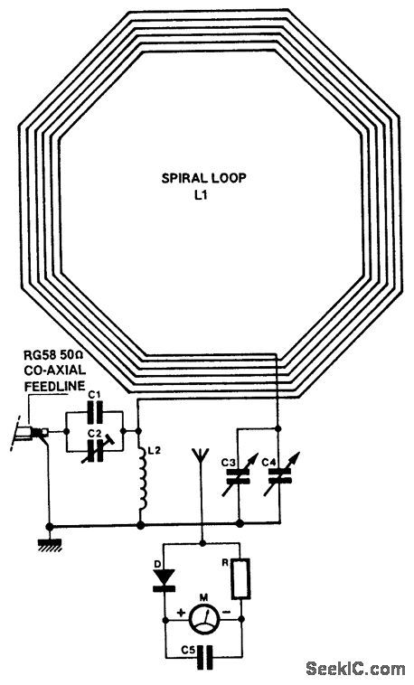


C1=3750 pF 500 V siver-mica capacitor.C2=100 pF preset capacitor(Jackson C803)C3=75 pF variable capacitor(Jackson C809),plus knob.C4=12.7 pF variable capacitor(Jackson C16),plus knob.C5=22 nF mica capacitor.M=250 μA f.s.d.40×40 mm moving coil meter(Maplin LB8O8).D=HF silicon diode.R=1 kΩ resistor(see text).L1=51/8 turns of PVC covered stranded 7/O.2 mm wlre,Outside diameter:1.2mm,1 kV/1.5 A rating(see text)L2=13 turns 16SWG tinned wlre,1 inch internal diameter.Feedline=48 inch RG58 coaxial cable,plus plug to suit transmitter.Box=ABS box type MB3,118×96×45 mm Maplin ref LH22.Terminal blocks=qty,412-way 2 amp terminal block Maplin ref,FE78.Spacers=qty.3 insulated spacer type M3,30 mm long,Mapin ref.FS4OT.Spokes=qty.48-foot lengths of 5/8×l/4inch molded hardwood(DIY store).Vertical support=23×O.8×0,Sinch wood(DIY store).Wood base=12×8×0.5 inch plywood or simiar.21/2 inch steel support bracket.
1. 4 lengths molded hardwood 3O x 5/8 x 1/4 Varnished. 2BA holes drilled in the centre. Glued and bolted together.2. 8 off 6-way 2-amp polythene terminal blocks used as insulated wire spacers.3. 51/8 turns of PVC stranded wire (for specs see component, list).4. See Fig. 3.5. Wood vertical support 23 x0.8 x0.8 , wood stained.6. 2 x 2BA bolt.7. Box front vertical support, 41/2 x 1/2 x 3/4 , wood stained.8. Wood base 12 x 8 x1/2 (for similar), wood stained.9. 21/2 steel support bracket behind wood vertical support.10. Drilled and secured with glue and c/s wood screws.Note: = inch=2.54cm.
Suitable for receiving or transmitting (10 W or less) on the 80-m band, this loop antenna might be helpful when an outside antenna is not possible. (View)
View full Circuit Diagram | Comments | Reading(1273)
LINE_OPERATED_AMPLIFIER
Published:2009/7/21 1:20:00 Author:Jessie
Push-pull phase shifter. single-ended preamp, and push-pull class B power amplifier all obtain supply voltages from AC supply that can either use power transformer or operate directly from line with diode rectifiers. Power output is enough to drive size 18 servomotor at 10W. Larger servomotors can be used if reduced supply voltages can be tolerated. Suitable power supply circuits are given.-A. Pshaenich, Servo Motor Drive Amplifiers, Motorola, Phoenix, AZ, 1972, AN-590. (View)
View full Circuit Diagram | Comments | Reading(0)
RANGING_SYSTEM
Published:2009/7/8 23:19:00 Author:May

Combine an electrostatic transducer with an ultrasonic transceiver IC to build a ranging system that senses objects at distances from 4 inches to more than 30 feet. Transducer Y1's broadband characteristic simplifies tuning. The secondary of T1 resonates with the 500-pF capacitor C1 at a frequency between 50 and 60 kHz. You tune L1 to this frequency by using an oscilloscope to note the maximum echo sensitivity at pin 1. Step-up transformer T1 prov.ides 150-V bias for the transducer. (View)
View full Circuit Diagram | Comments | Reading(690)
| Pages:924/2234 At 20921922923924925926927928929930931932933934935936937938939940Under 20 |
Circuit Categories
power supply circuit
Amplifier Circuit
Basic Circuit
LED and Light Circuit
Sensor Circuit
Signal Processing
Electrical Equipment Circuit
Control Circuit
Remote Control Circuit
A/D-D/A Converter Circuit
Audio Circuit
Measuring and Test Circuit
Communication Circuit
Computer-Related Circuit
555 Circuit
Automotive Circuit
Repairing Circuit