
Circuit Diagram
Index 922
0_13_V_AT_40_mA
Published:2009/7/8 23:37:00 Author:May

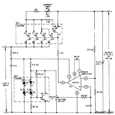
Cornbination of RCA CA3130 opamp and two CA3086 NPN transistor arrays provides better than 0.01% regulation from no Ioad to full Ioad and input regulation of 0.02%/ V. Hum and noise output is less than 25 μV up to 100 kHz.- Linear Integrated Circuits and MOS/FET's, RCA Solid State Division, Somer-ville, NJ, 1977, p 236-243. (View)
View full Circuit Diagram | Comments | Reading(773)
CONDUCTIVITY_METER
Published:2009/7/20 20:57:00 Author:Jessie

Circuit using single quad opamp measures relative change in con-centration of salt solution by monitoring its conductance. Use of alternating current through solution eliminates errors caused by electrolysis effect. Wien-bridge oscillator having R4C1 and R4R3 as arms of bridge generates 1-kHz signal for driving amplifier A2 through solution. P1 controls oscillator amplitude, and P2 adjusts gain of A2. A3-A4 form precision rectifier giving output voltage equal to absolute value of input voltage.-M. Ahmon, One-Chip Conductivity Meter Monitors Salt Concentration, Electronics, Sept. 15, 1978, p 132-133. (View)
View full Circuit Diagram | Comments | Reading(9830)
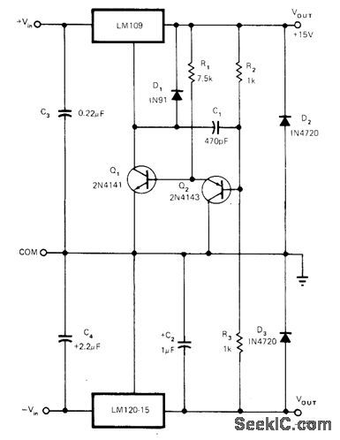
±15_V_WITH_TRACKING
Published:2009/7/8 23:35:00 Author:May


In arrangement shown for National regulator ICs, positive output voltage tracks negative voltage to better than 1%. Ripple rejection is 80 dB for both outputs. Load regulation is 30 mV at 1 A for nega-tive outputand less than 10 mV for positive output. Circuit works well for output in range of 16 to ±15 V. C, provides stability.-C. T. Nel-son, Power Distribution and Regulation Can Be Simple, Cheap and Rugged, EDN Magazine, Feb. 20, 1973, p 52-58. (View)
View full Circuit Diagram | Comments | Reading(599)
LOW_COST_CRYSTAL_FILTERS
Published:2009/7/8 23:35:00 Author:May

Low-cost CB crystals can be used for these 9-MHz crystal ladder filters. Notice that the 27-MHz crystals (3rd overtone) are used on their fundamental frequencies. (View)
View full Circuit Diagram | Comments | Reading(2261)
CONDUCTIVITY_METER
Published:2009/7/20 20:57:00 Author:Jessie
Circuit using single quad opamp measures relative change in con-centration of salt solution by monitoring its conductance. Use of alternating current through solution eliminates errors caused by electrolysis effect. Wien-bridge oscillator having R4C1 and R4R3 as arms of bridge generates 1-kHz signal for driving amplifier A2 through solution. P1 controls oscillator amplitude, and P2 adjusts gain of A2. A3-A4 form precision rectifier giving output voltage equal to absolute value of input voltage.-M. Ahmon, One-Chip Conductivity Meter Monitors Salt Concentration, Electronics, Sept. 15, 1978, p 132-133. (View)
View full Circuit Diagram | Comments | Reading(0)
PHOTOCELL_BRIDGE
Published:2009/7/8 23:34:00 Author:May
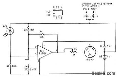

Radio Shack 276-116 cadmium sulfide photocell is connected in Wheatstone bridge circuit. When bridge is bal-anced, RS741C opamp connected to opposite comers of bridge receives no voltage and meter reads zero. Light on photocell unbalances bridge and gives meter deflection. Can be used as high-sensitivity light meter. Adjust R3 until meter reads zero with photocell covered while R5 is at maximum resistance,adjust R5 until needle moves away from zero,rezero with R3,and repeat procedure until meter can no longerbe brought to zero,Sensitivityis now maximum,and uncovered photocell Will detectfiame from candle at 20 feet.-F.M.Mims,''Integrated Circuit Projects,vol 4,''Radio Shack,Fort Worth,TX,1977,2nd Ed.,p 29-35.
(View)
View full Circuit Diagram | Comments | Reading(1196)
_12_V_AT_2_A
Published:2009/7/8 23:34:00 Author:May
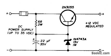
Developed for unregulated 12-VDC supplies used by some amateurs with low-power VHF FM equipment, where no-load voltage may be 18 V or more. During transmit, voltage drops to about 12V, but on receive may exceed voltage ratings of small-signal transistors in transceiver. Use heatsinkwith transistor, and use 2-A fuse to protect transistor from shorted load.-J. Fisk, Circuits and Techniques, Ham Radio, June 1976, p 48-52. (View)
View full Circuit Diagram | Comments | Reading(515)
POSITIVE_SHUNT_REGULATION
Published:2009/7/8 23:34:00 Author:May

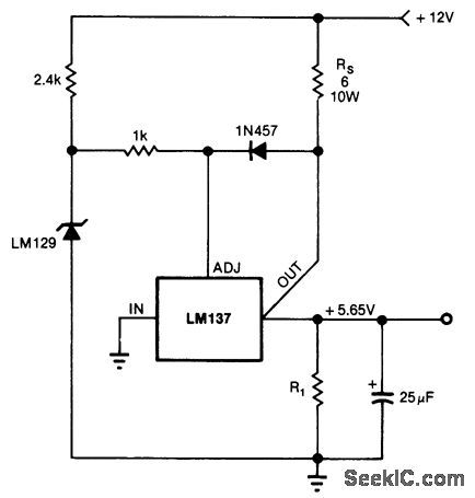
Connection shown for LM137 negative series regulator provides high-reliability positive shunt regulation for applications having high-voltage spike on raw DC supply. Output is 5.65 V.-P. Lefferts, Series Regulators Provide Shunt Regulation, EDNMagazine, Sept.5, 1978, p 158 and 160. (View)
View full Circuit Diagram | Comments | Reading(584)
VIDEO_DISTRIBUTION_AMPLIFIER
Published:2009/7/20 20:56:00 Author:Jessie

Bandwidth is 12 Mc, for high-resolution closed-circuit television and high-speed facsimile systems. Input level is 2 v and output level is 5 v for 75.ohm lines. Differential amplifier eliminates second harmonic distortion without use of interstage transformers.-H. H. Naidich, Video Distribution Amplifier Eliminates Interstage Transformers, Eectronics, 34:24, p 58-61.
(View)
View full Circuit Diagram | Comments | Reading(0)
20_kHz_ARC_WELDING_INVERTER
Published:2009/7/8 23:33:00 Author:May


The Class A series resonant inverter portrayed is well-known and respected for its high efftciency, low cost, and small size, provided that operating frequency is greater than about 3 kHz. The disadvantages are, at least in high power versions, the difftculty in effecting smooth RFI-free output voltage modulationwithout significant added complexity, and a natural tendency to run away under no-load (highQ) conditions.The 20-kHz control circuit (see Fig. 2) overcomes these shortcomings by feeding back into the asymmetrical thyristor trigger pulse generators (see Fig. 3) signals that simultaneously shut the inverter down, when its output voltage exceeds a preset threshold, then time-ratio modulates the output. This feedback is accomplished with full galvanic isolation between input and output thanks to an H11L opto-Schmitt coupler. The fundamental 20-kHz gate firing pulses are generated by a PUT relaxation oscillator Q1. The pulses are then amplified by transistors Q2 and Q3. The 20-kHz sinusoidal load current flowing in the pri-mary of the output transformer is then detected by current transformer CT1, with op amp A1 converting the sine wave into a square wave, whose transitions coincide with the load current zero points.Consequently, each time the output current changes, phase A1 also changes state and, via transistor Q4, either connects the thyristor gate to a -8 Vdc supply for minimum gate assisted turn-off time and highest reapplied dVldt capability or disables this supply to prepare the thyristor for subsequent firing.Modulation intelligence is coupled into this same H11L through two additional PUTs, Q6 and Q7, Q6 oscillates at a fixed 1.25 kHz, which establishes the modulation frequency. The duty cycle is determined by a second oscillator, Q7, whose conduction state, on or off, establishes or removes current from the H11L diode. With afundamental inverter frequency of 20 kHz and a modulation frequency of 1.25 kHz, the resultant time ratio-controlled power output is given by:where PM= 100% continuous output power. Minimum power is one cycle of 20 kHz (50 μs) in the 1.25-kHz modulation frame (800 μs), that is, 6.25% PM. (View)
View full Circuit Diagram | Comments | Reading(5196)
TUNABLE_BANDPASS_FILTER
Published:2009/7/8 23:33:00 Author:May

One of the difficulties in the design of higher-order tunable bandpass filters is achieving correct track-ing of the variable resistors in the RC networks. The use of switched capacitor networks can obviate that difficulty, as is shown in this filter.
The filter can be divided roughly into two stages: an oscillator that controls the electronic switches and the four phase-shift networks that provide the filtering proper. The oscillator, based on a 555, generates a pulsating signal whose frequency is adjustable over a wide range: the duty factor varies from 1:10 to 100:1.
Electronic switches ES1 through ES4 form the variable resistors whose value is dependent on the frequency of the digital signal. The operation of these switches is fairly simple. When they are closed, their resistance is about 60Ω; when they are open, it is virtually infinitely high. If a switch is closed for, say, 25% of the time, its average resistance is therefore 240Ω. Varying the open:closed ratio of each switch varies the equivalent average resistance. The switching rate of the switches must be much greater than the highest audio frequency to prevent audible interference between the audio and the clock signals.
The input signal causes a given direct voltage across C1, so the op amp can be operated in a quasisym-metric manner, in spite of the single supply voltage. The direct voltage is removed from the output signal by capacitor C10.
The fourth-order filter in the diagram can be used over the entire audio range and it has an ampliftca-tion of about 40, although this depends to some extent on the clock frequency. The bandwidth depends mainly on the set frequency. The circuit draws a current of not more than 15 mA. (View)
View full Circuit Diagram | Comments | Reading(4427)
Precision_10_volt_reference_with_fine_trim_adjustment
Published:2009/7/20 20:56:00 Author:Jessie
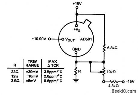
Precision 10-volt reference with fine trim adjustment (courtesy Analog Devices, Inc.). (View)
View full Circuit Diagram | Comments | Reading(609)
LAMP_DRIVE
Published:2009/7/20 20:55:00 Author:Jessie
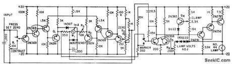
Count-rate meter of radiation-detecting tumor stunner provides input signal for d-c amplifier. Controls R1 and R2in difference amplifier provides zero suppression and R3 provides scale expansion. Circuit drives lamp that exposes film in step with scanning motion of probe.-E. Gordy and G. Sieber, Sensitive Amplifier Helps Lo-Gale Tumors, Electronics, 34:1, p 123-124. (View)
View full Circuit Diagram | Comments | Reading(619)
PROGRAMMABLE_FREQUENCY_SINE_WAVE_OSCILLATOR
Published:2009/7/9 1:26:00 Author:May

This Wien-bridge oscillator is very popular for signal generators, since it is easily turned over a wide frequency range, and has a very low distortion sine-wave output. The frequency determining networks can be designed from about 10 Hz to greater than 1 MHz; the output level is about 6.0-V rms. By substituting a programmable attenuator for the buffer amplifier, a very versatile sine-wave source for automatic testing, etc. can be constructed.
(View)
View full Circuit Diagram | Comments | Reading(801)
POT_TESTER
Published:2009/7/20 20:55:00 Author:Jessie

Developed for testing noisy 10K wirewound linear pots used in control of theatrical lighting system. Circuit detects any mo-mentary open and drives LED to produce visible flash lasting about 0.1 s. Circuit operates from -10 V provided by bridge and AC transformer.Left half of IC1 acts as comparator whose out-put stays low as long as input is above thresh-old voltage. When pot passes open point, pin 5 goes high and charges C3, making right half of IC1 turn on LED.-C. J. Shakespeare, Test Your Pot, Modem Electronics, Oct. 1978, p 38-39. (View)
View full Circuit Diagram | Comments | Reading(664)
SUMMING_AMPLIFIER_CLAMPING_CIRCUIT
Published:2009/7/9 1:26:00 Author:May
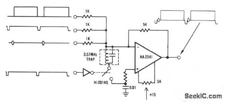
This circuit is a traditional summing amplifier configuration with the addition of the dc clamping circuit The operation is quite simple; each component-synchro nization, color burst, picture information, etc.-of the composite video signal is applied to its own input terminal of the amplifter. These signals combine algebraically and form the composite signal at the output. The clamping circuit, if used, restores the 0-V reference of the composite signal. (View)
View full Circuit Diagram | Comments | Reading(970)
SCR_FOR_HORIZONTAL_OUTPUT
Published:2009/7/20 20:54:00 Author:Jessie
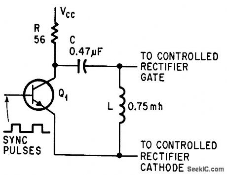
Sync pulses saturate driver Q1, permitting C to charge, for achieving fast turnoff after pate-turnoff scr conducts yoke current for 27 microsec to defect electron beams.-L. D. Shergalis, Scr's for 19-Inch Tv, Electronics, 37:23, p 97-98. (View)
View full Circuit Diagram | Comments | Reading(606)
DUAL_GATE_MOSFET_RF_AMP_STAGE
Published:2009/7/9 1:25:00 Author:May
The use of a double-tuned input and a single-tuned output yield superior RF selectivity to that of equivalent single-tuned designs. AGC, if required, can be added to gate 2 of Q1, and should drive gate 2 negative for decreased gain. (View)
View full Circuit Diagram | Comments | Reading(1659)
HC_BASED_OSCILLATORS
Published:2009/7/9 1:24:00 Author:May

Two inverters, one resistor, and one capacitor are all that is required to make a HC(T)-based oscillator that gives reliable operation up to about 10 MHz. The use of two HC inverters produces a fairly symmetrical rectangular output signal. In the same circuit, HCT inverters give a duty factor of about 25%, rather than about 50%, since the toggle point of an HC and an HCT inverter is 1/2 VCC, and slightly less than 2 V, respectively. If the oscillator is to operate above 10 MHz, the resistor is replaced with a small inductor, as shown in Fig.68-4B.
The output frequency of the circuit in Fig. 68-4A is given as about 1/1.8rc, and can be made variable by connecting a 100-KΩ potentiometer in series with R. The solution adopted for the oscillator in Fig. 68-4B is even simpler: C is a 50-pF trimmer capacitor.
(View)
View full Circuit Diagram | Comments | Reading(760)
Current_boost_regulator_for__5_volts_at_4_amperes_with_5_ampere_current_limiting
Published:2009/7/20 20:54:00 Author:Jessie
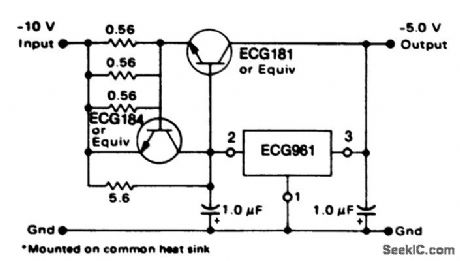
Current boost regulator for -5 volts at 4 amperes with 5-ampere current limiting. When a boost transistor is used short-circuit current is equal to the sum of the series pass and regulator limits, which are measured at 3.2 amperes and 1.8 amperes respectively. Series pass limiting is approximately equal to 0.6 volts/RSC (courtesy GTE Sylvania Incorporated). (View)
View full Circuit Diagram | Comments | Reading(624)
| Pages:922/2234 At 20921922923924925926927928929930931932933934935936937938939940Under 20 |
Circuit Categories
power supply circuit
Amplifier Circuit
Basic Circuit
LED and Light Circuit
Sensor Circuit
Signal Processing
Electrical Equipment Circuit
Control Circuit
Remote Control Circuit
A/D-D/A Converter Circuit
Audio Circuit
Measuring and Test Circuit
Communication Circuit
Computer-Related Circuit
555 Circuit
Automotive Circuit
Repairing Circuit