Basic Circuit
AUDIO_FREQUENCY_DOUBLER
Published:2009/7/8 23:44:00 Author:May | From:SeekIC


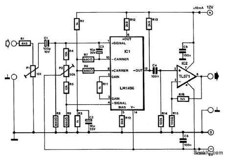
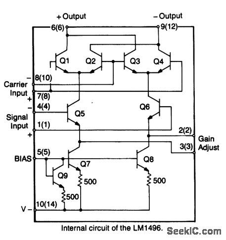
Often the frequency of a signal must be dou-bled: modulator/demodulator chip LM1496 is an ideal basis for this.
From trigonometry it is well known that:
2sitvrcosx= sin2x
and∶
sin2=1-xcos2x.
These equations indicate that the product of two pure sinusoidal signals of the same frequency is one signal of double that frequency. The purity of the original signals is important: composite signals would give rise to all sorts of undesired products.
The LM1496 can only process signals that are not greater than 25 mV: above that level, serious distortion will occur. The design is therefore pro-vided with a potential divider at its input. This addi-tion makes it possible, for instance, to arrange for a 500-mV input signal to result in a signal of only 25 mV at the input of the LM1496.
To provide a sufficiently high output signal, the output of IC1 is magnified by op amp IC2, which is connected as a noninverting amplifier. Because the output of IC1 contains a dc component of about 8 V, the coupling between the two stages must be via a capacitor, C4.
With values of R15 and R16 as shown, IC2 gives an amplification of 16 (24 dB). The overall amplifica-tion of the circuit depends on the level of the input signal: with an input of 1.2 V, the amplification is unity; when the input drops to 0.1 V, the amplification is just 0.1. The value of the input resistors has been fixed at 6800: this value gives a reasonable compromise between the requirements for a high input impedance and a low noise level.
To ensure good suppression of the input signal at the output, the voltages at pin 1 and pin 4 of IC1 must be absolutely identical to P4. It is possible, with the aid of a spectrum analyzer, to suppress the fundamental (input) frequency by 60 to 70 dB.
The output signal at pin 12 is distorted easily, because the IC is not really designed for this kind of operation. The distortion depends on the level of the input signal. At a frequency of 1 kHz and an input level of 100 mV, the distortion is about 0.6%; when the input level is raised to 500 mV, the distortion increases to 2.3%, and when the input level is 1 V, the distortion is 6%. The signal-to-noise ratio under these conditions varies between 60 and 80 dB.
The circuit draws a current of 10 mA from the positive supply line and 5 mA from the negative line.The phase shift between the input and output signals is about 45° (output lags). Finally, although the nor-mal output is taken from pin 12, a similar output that is shifted by 180° (with respect to that at pin 12), is available at pin 6.
Reprinted Url Of This Article:
http://www.seekic.com/circuit_diagram/Basic_Circuit/AUDIO_FREQUENCY_DOUBLER.html
Print this Page | Comments | Reading(3)

Article Categories
power supply circuit
Amplifier Circuit
Basic Circuit
LED and Light Circuit
Sensor Circuit
Signal Processing
Electrical Equipment Circuit
Control Circuit
Remote Control Circuit
A/D-D/A Converter Circuit
Audio Circuit
Measuring and Test Circuit
Communication Circuit
Computer-Related Circuit
555 Circuit
Automotive Circuit
Repairing Circuit
Code: