
Circuit Diagram
Index 910
PHOTOREED
Published:2009/7/20 12:07:00 Author:Jessie

Combines resonant reed relay with photosensor to give frequency-sensitive control in which switching of contacts is accomplished by electro-optical techniques. Photosensor is exposed to intermittent light when reed vibrates like shutter between lamp and sensor.-Frequency-Sensitive Control Uses Light, Electronics, 34:36, p 88-91. (View)
View full Circuit Diagram | Comments | Reading(826)
EYE_MOTION_MVBR_CHAIN
Published:2009/7/20 12:06:00 Author:Jessie

Illuminated photocell triggers mvbr chain. Starter-mvbr is triggered by positive pulse on grid of V1A, but remaining mvbr stages are triggered by negative pulse on cathode. Output pulses are taken from across 6,800-ohm resistor and a-c coupled to gate.-E. L. Thomas, R. Howat, and N. H. Mackworth, Tv Tracker Records Eye Focus Points, Electronics, 33:17, p 57-59. (View)
View full Circuit Diagram | Comments | Reading(613)
MULTIVIBRATOR_WITHLEDS
Published:2009/7/9 2:15:00 Author:May
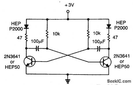
A simple astable multivibrator IS used to alternately flash two LEDs.The approximate time constant is 0.69.
(R1C1+R2C2) R1=R2=10 kΩ C1=C2=100μF (View)
View full Circuit Diagram | Comments | Reading(772)
PROJECTILE_GLOW_DETECTOR
Published:2009/7/20 12:05:00 Author:Jessie

2N469A phototransistor detects brief low-intensity self-luminous shroud of projectile, and feeds high-gain pulse amplifier that elevates voltage enough to ionize thyratron that initiates discharge of spark-source capacitor for shadowgraph photography.-O. H. Bock and P. L. Clemens, Aerodynamic Measurements in a Hypervelocity Gun Range, Electronics, 34:44, p 33-37. (View)
View full Circuit Diagram | Comments | Reading(708)
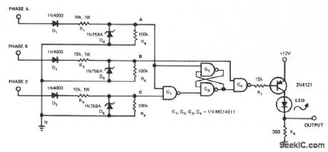
PHASE_DETECTOR
Published:2009/7/9 2:15:00 Author:May


The output of the detector contains a term related to the cosine of the phase angle. Two signals of equal frequency are applied to the inputs. The frequencies are multiplied together, producing the sum and difference frequencies. Equal frequencies cause the difference component to become dc, while the undesired sum component is ftltered out. The dc component is related to the phase angle by the graph of Fig.70-2B. At 90°, the cosine becomes zero, while being at maximum positive or maximum negative at 0°and 180°, respectively. The advantage of using the balanced modulator over other types of phase comparators is the excellent conversion linearity. This configuration also provides a conversion gain, rather than a loss for greater resolution. Used in conjunction with a phase-locked loop, for instance, the balanced modulator provides a very low-distortion FM demodulator.
Correct phase sequences (ABC, BCA, or CAB) produce trains of output pulses and illuminate the LED. The output stays low and the LED remains dark for incorrect sequences (BAC, ACB, or CBA) or for phase loss (phase A, B, or C missing). (View)
View full Circuit Diagram | Comments | Reading(2054)
LIGHT_SOURCE_STABILIZER
Published:2009/7/20 11:50:00 Author:Jessie

Feedback circuit generates precise pulses to control light level of photoelectric light source. Difference between reference current supplied by zener diode and current from photocell is amplified by transistor chain and applied to Q6 to adjust lamp current.-J. R. Dyke, Illumination Stabilizer for Photosensing System, Electronics, 34:52, p 44-45. (View)
View full Circuit Diagram | Comments | Reading(1074)
PAL_NTSC_DECODER_WITH_RGB_INPUTS
Published:2009/7/9 2:14:00 Author:May
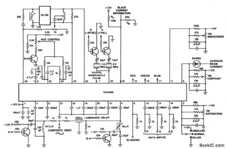
This circuit shows the TDA3566 for a PAL/NTSC Decoder. (View)
View full Circuit Diagram | Comments | Reading(2549)
MEASURING_FLASHES
Published:2009/7/20 11:46:00 Author:Jessie

Measures and holds intensity of single flash or total value of series of flashes.-C. R. Kerns, FET Circuit Stores Light Measurement, Electronics, 38:22, p 66. (View)
View full Circuit Diagram | Comments | Reading(712)
PHASE_SEQUENCE_DETECTOR
Published:2009/7/9 2:13:00 Author:May

View full Circuit Diagram | Comments | Reading(0)
SINGLE_COLD_CATHODE_AMPLIFIER
Published:2009/7/20 11:45:00 Author:Jessie

Actuates thermal relay directly from photoconductive cell, for turning on lights at sunset.-P. Bergweger, Photoelectric Control Using Cold Cathode Amplifiers, Electronics, 33:27, p 46-47. (View)
View full Circuit Diagram | Comments | Reading(1058)
CONVEYOR_LINE_JAM_DETECTOR
Published:2009/7/20 11:44:00 Author:Jessie

Interruption of light beam to light-activated scr for more than few millisec fires SCR1, opening relay. Momentary interruptions by objects moving normally on conveyor have no effect. Circuit resets automatically when light is restored.-E. K. Howell, Light-Activated Switch Expands Uses of Silicon-Controlled Rectifiers, Electronics, 37:15, p 53-61. (View)
View full Circuit Diagram | Comments | Reading(1435)
SEQUENTIAL_LED_FLASHER_WITH_REVERSIBLE_DIRECTION
Published:2009/7/9 2:13:00 Author:May

A 555 timer clocks a 74190 up/down counter. The 74190 drives BCD decoder driver 7442. The 7476 is used to reverse the count on 0 and 9, which results in an up-down-up-down count sequence. (View)
View full Circuit Diagram | Comments | Reading(6023)
6_W_AUDIO_AMPLIFIER_WITH_PREAMP
Published:2009/7/9 2:12:00 Author:May


This monolithic IC, class-B, audio amplifter circuit is a 6-W car radio amplifter for use with 4-Ω and 2- Ω load impedances. (View)
View full Circuit Diagram | Comments | Reading(815)
PHASE_SELECTOR_PHASE_DETECTOR_SYNCHRONOUS_RECTIFIER_BALANCED_MODULATOR
Published:2009/7/9 2:12:00 Author:May


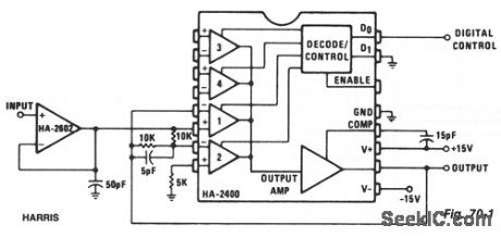
This circuit passes the input signal at unity gain, either unchanged or inverted, depending on the digital control input. A buffered input is shown, since low-source impedance is essential. Gain can be added by modifications to the feedback networks. Signals up to 100 kHz can be handled with 20.0-V pk-pk, output.The circuit becomes a phase detector when driving the digital control input with a reference phase at the same frequency as the input signal; the average dc output is proportional to the phase difference, with 0 V at +90°. By connecting the output to a comparator, which in turn drives the digital control, a synchronous full-wave rectifier is formed. With a low-frequency input signal and a high-frequency digital control signal, a balanced (suppressed carrier) modulator is formed. (View)
View full Circuit Diagram | Comments | Reading(1390)
COMPOSITE_VIDEO_SIGNAL_TEXT_ADDER
Published:2009/7/9 2:11:00 Author:May
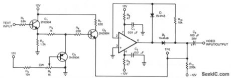
This circuit shows a simple way to add text information to a composite-video signal that might be floating at some indeterminate dc level. The text generator and composite-video source must have the same sync signal. The video-input and -output signals share the same terminal. C3 couples the video signal to the output of a rectifier circuit that is based on a subvideo-speed op amp. A faster op amp would clamp on individual sync pulses rather than on the video waveform's average value, as is desired. R11 serves as a pulldown resistor and feedback resistor R10 ensures that TP6 remains at ground level. Emitter follower Q1 buffers the text signal, and R5 serves as a gain control. A simple clamp circuit, Q2, is sufficient for regulating amplitude, because the text signal contains no gray-scale levels. Q3 couples the text signal into the op-amp clamp circuit. (View)
View full Circuit Diagram | Comments | Reading(1475)
AUDIO_POWER_AMPLIFIER
Published:2009/7/9 2:08:00 Author:May

he single speaker amplifier circuit uses cur-rent feedback, rather than the more popular voltage feedback. The feedback loop is from the junction of the speaker terminal and a 0.5-Ω resistor, to the inverting input of the NE5534. When the input to the amplifier is positive, the power supply supplies current through the TIP32 and the load to ground.Conversely, with a negative input, the TIP31 sup-plies current through the load to ground. The gain is set to about 15 (gain SPKR 8 Ω/0.5 Ω feed-back). The 0.22-μF capacitor across the speaker rolls off its response beyond the frequencies of interest. Using the 0.22-μF capacitor specified, the amplifier current output is 3 dB down at 90 kHz where the speaker impedance is about 20 Ω. To set the recommended class A output collector current, adjust the value of either 130-Ω resistor. An output current of 50 to 100 mA will provide a good operating midpoint between the best crossover distortion and power dissipation. (View)
View full Circuit Diagram | Comments | Reading(0)
CELL_GROWTH_MICROPHOTOMETER
Published:2009/7/20 11:35:00 Author:Jessie

Permits direct measurement of transmittance while stained cells are studied visually at magnification of 1,000 X. Beam-splitting mirror sends 90% of light to multiplier phototube. Maximum current sensitivity is 0.01 microamp full scale.-E. Gordy, Microphotometer Aids Biologists, Electronics, 32:28, p 62-64. (View)
View full Circuit Diagram | Comments | Reading(564)
CRO_DOUBLER
Published:2009/7/9 2:07:00 Author:May

IC1a, IC1b, and IC1c of the quad two-input NAND gate 4011 are connected as an astable multivibrator; IC1d is connected as an inverter. Terminals 3 and 11 of the 4011 produce square waves wit opposite phases. The square waves, ep, at the output of IC1a, passing through differentiator C4R13, then form positive and negative pulses, et. The dual op amps of the LM358 ar, used as two gated amplifiers for singles e1and e2 and fed through terminals 2 and 6, to be displayed simultaneously on the CRO screen.
The two opposite-phase square waves ep, and ep are used to gate IC2a and IC2b at terminals 3 and 5 of the LM358, respectively. Resistances R9 and R10 are preadjusted so that one op amp is driven to saturation while the other works normally as an amplifier. Thus, they will amplify signals e1 and e2 alternately, and two separate traces will be displayed on the screen. Resistance R12 can be varied to adjust the vertical separation of the two traces.
Select a suitable value for C1 with switch S, and adjust the pot of R1. The frequency of square waves can be varied from 1 to 106 cps. This process is necessary for stabilizing the waveforms dtsptiyed on the screen. A common supply of 6 V is used in the circuit.
(View)
View full Circuit Diagram | Comments | Reading(1386)
PHOTOCELLS_PROVIDE_NOISE_FREE_AUDIO_KEYING
Published:2009/7/20 11:30:00 Author:Jessie

Photoresistors R5 and R6 isolate control function from signal circuit to avoid switching transients. S1 may be replaced by automatic pulsing circuit.-A. Martens, Noise-Free Keying Circuit, Electronics, 35:13, p 53. (View)
View full Circuit Diagram | Comments | Reading(1098)
CLASS_D_POWER_AMPLIFIER
Published:2009/7/9 2:06:00 Author:May

In this circuit, a 2-MHz clock is divided by eight ht U1, providing a stable 250-kHz carrier. Q1 and Q2 buffer the clock and provide a low-impedance drive for op amp U4, which is a high-gain amplifier and integrator. U4 accepts audio inputs and converts the 250-kHz square wave into a triangular wave. The summed audio and triangular-wave signal is applied to the input of comparator U7, where it is compared with a dc reference to produce a pulse-width modulated signal at the output of U7.The output devices switch between the + 50 V and -50 V rails in a complementary fashion, driving the output filter that is a sixth-order Butterworth low-pass type, which demodulates the audio and attenuates the carrier and high frequency components.Feedback is provided Rf; amplifier gain is RfRi.
Specifications: 200 W continuous power into a 4-Ω load; 20 to 20 kHz frequency response +0.5, -1.0 dB at 200 W; TED, IMD 0.5% at 200 W; 1.5-V rms input for rated output; 69 dB S/N ratio, A weighting; 6.6-V ms slew rate. (View)
View full Circuit Diagram | Comments | Reading(3974)
| Pages:910/2234 At 20901902903904905906907908909910911912913914915916917918919920Under 20 |
Circuit Categories
power supply circuit
Amplifier Circuit
Basic Circuit
LED and Light Circuit
Sensor Circuit
Signal Processing
Electrical Equipment Circuit
Control Circuit
Remote Control Circuit
A/D-D/A Converter Circuit
Audio Circuit
Measuring and Test Circuit
Communication Circuit
Computer-Related Circuit
555 Circuit
Automotive Circuit
Repairing Circuit