Basic Circuit
PICTURE_FIXER_INVERTER
Published:2009/7/9 2:36:00 Author:May | From:SeekIC

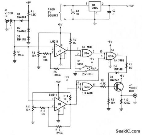
The circuit will accept a video signal, separate the sync pulses, invert the video, and add new video to the old sync pulses. The video signal is brought in through J1 and applied to a clamping circuit consisting of C1, D1, D2, D3, R1, and R2. The clamp circuit forces all of the sync pulses to align with the same dc voltage level. With the video voltage clamped, the trip points of the comparators that follow can be set with trimmer resistors R3 and R11. The resistors will not have to be readjusted. One comparator, U1, is adjusted to change states with a change in either video or sync-pulse levels. The other comparator, U2, is adjusted to trip on changes of sync-pulse levels only.The output of U1 now consists of a logic level, 0 to + 5 V, signal that contains both sync pulses and video. The composite signal is coupled to an EXCLUSIVE-OR gate, U3a, where it is either inverted or not inverted, depending upon the position of switch NORM/REV S1. The output, at pin 3 of U3a, is next sent to U3b. There the composite signal is combined with the sync-pulse only signal from U2. The EXCLUSIVE-OR action of U3b cancels out the sync pulses, leaving only video at the IC's output.Since the sync pulses are inverted as they pass through U2, they must be inverted once more before being combined with the video signal. That final inversion is performed by U3c, and that device's output is combined with that of U3b via D4, R7, R8, and R9. The newly combined signal is buffered by emitter-follower Q1, and sent to the outside world via J2. The circuit can be powered by a 9- to 12-V wall-mount power supply. The supply voltage is regulated down to 5 V by U4.
Reprinted Url Of This Article:
http://www.seekic.com/circuit_diagram/Basic_Circuit/PICTURE_FIXER_INVERTER.html
Print this Page | Comments | Reading(3)

Article Categories
power supply circuit
Amplifier Circuit
Basic Circuit
LED and Light Circuit
Sensor Circuit
Signal Processing
Electrical Equipment Circuit
Control Circuit
Remote Control Circuit
A/D-D/A Converter Circuit
Audio Circuit
Measuring and Test Circuit
Communication Circuit
Computer-Related Circuit
555 Circuit
Automotive Circuit
Repairing Circuit
Code: