Amplifier Circuit
PHOTODIODE_SOURCE_FOLLOWER
Published:2009/7/8 22:58:00 Author:May | From:SeekIC

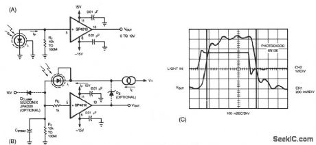
A common method of transforming the output current of a photodiode into a voltage signal, paralleling the photodiode with a high-value load resistor, produces a nonlinear response. Also the combination of the load's transresistance, RT, and the photodiode's junction capacitance, CJ, slows the circuit's response time. Figure 67-11B shows virtually the same components as Fig. 67-11A rearranged to maximize the inherent speed and linearity of the photodiode. The SP4010 (available from Hybrid Systems, Billerica, MA) is a unity voltage-gain buffer with a JFET input, 60-MHz 3-dB bandwidth, and 18-bit, 0.0004%, line-arity over a ± 10 V input range.
In the circuit of Fig. 67-11B, the photodiode sees a constant voltage across its terminals, which is essential for linear photodiode outputs. The optional zener diode, DZ, sets a reverse bias at the photo-diode for lower junction capacitance and higher speed. If y
ou don't use DZ, be sure to connect the feed-back loop. An optional diode, DCLAMP, limits the output in case of unexpected light bursts, but results in increased dark-current leakage and lower speed. The buffered output of the circuit equals the photodiode current times the transresistance, RT. Figure 67-11C shows the circuit's response to a fast light pulse.
Reprinted Url Of This Article:
http://www.seekic.com/circuit_diagram/Amplifier_Circuit/PHOTODIODE_SOURCE_FOLLOWER.html
Print this Page | Comments | Reading(3)

Article Categories
power supply circuit
Amplifier Circuit
Basic Circuit
LED and Light Circuit
Sensor Circuit
Signal Processing
Electrical Equipment Circuit
Control Circuit
Remote Control Circuit
A/D-D/A Converter Circuit
Audio Circuit
Measuring and Test Circuit
Communication Circuit
Computer-Related Circuit
555 Circuit
Automotive Circuit
Repairing Circuit
Code: