
Circuit Diagram
Index 1398
High-precision measurement amplifier circuit composed of the INA131
Published:2011/6/27 1:51:00 Author:Rebekka | Keyword: High-precision measurement amplifier

The INA131 is a low-cost general-purpose amplifier. Its inside gain resistor passes laser trimmed and makes the gain error small. It provides a standard gain of 100. The figure shows the high-precision measuring amplifier and the input signal of the electrical diagram bridge sensor (load cell, such as strain, displacement measurement sensors, etc.). This connection of the 50Hz power interference and high common mode interference rejection is very high. The magnification is 100, if you need a higher gain, you can add a gain resistor RG in ①, ⑧ foot indirectly. The gain size: G = 100 +250 kΩ / RG. (View)
View full Circuit Diagram | Comments | Reading(1075)
GENERAL_PURPOSE_IR_RECEIVER
Published:2009/6/19 4:18:00 Author:May

Suitable for amplitude-modulated IR beams, this receiver provides an audio signal that corresponds to the modulation envelope. Phototransistor Q1 should be properly mounted and shielded from stray light. This receiver should drive a small earphone dire (View)
View full Circuit Diagram | Comments | Reading(2397)
Wien bridge oscillator circuit controlled by photosensitive resistance
Published:2011/7/14 20:22:00 Author:zj | Keyword: Wien bridge, oscillator circuit, photosensitive resistance

This diagram is wien bridge oscillator circuit controlled by photosensitive resistance. Usually it uses lamp and FET tube for the stability of wien bridge oscillator circuit amplitude. When you use lamp, the amplitude dynamic range can increase. But the response speed will become slow. When you use FET tube, the response speed will increase. But the amplitube dynamic range will become narrow. As the circuit shown in the figue 6-3, the amplitude stabilized element adopts optical coupler MCD521H composed of LED and photosensitive resistance to solve the problem. This is a kind of fast response, wide dynamic range and no mechanical vibration influence, quality oscillation circuit.
(View)
View full Circuit Diagram | Comments | Reading(1194)
Operational amplifier all-function zero method circuit diagram
Published:2011/6/27 4:53:00 Author:Rebekka | Keyword: Operational amplifier all-function zero method
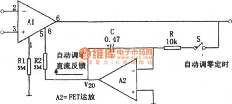
The figure shows the generic auto-zero circuit. A2 is the FET input type integrated chip. The integrator is composed of R, C, etc. It can be integrated to the DC output offset voltage. The switch S is an electronic switch that can automatically achieve the sampling time period. It can make the A1 output offset voltage be used as the input signal. The output points drive the zero end of A1, so that the offset voltage is the minimum state . The resistance of resistors R1 and R2 are larger. The different types of integrated operational amplifier values is around 5MΩ. (View)
View full Circuit Diagram | Comments | Reading(516)
ULTRASONIC_GLEANER
Published:2009/6/19 4:18:00 Author:May


An ultrasonic cleaner is useful to clean certain items. This circuit uses a microcontroller to con-trol timing and give a digital readout, but only the basic oscillator can be used, if desired. RES1, RES2 are piezoelectric transducers driven by power oscillator Q1. Q1 is powered by a bridge rectifier-capacitor input filter that operates directly off the ac line. The frequency is 40 to 60 kHz. (View)
View full Circuit Diagram | Comments | Reading(11026)
FM_INFRARED_RECEIVER_FOR_AUDIO_RECEPTION
Published:2009/6/19 4:17:00 Author:May

Modulated IR energy strikes Q2, a phototransistor. Q1 is a tunde amplifier,and feeds PLL detector U1.U2 is an audio amplifier that drives a speaker. (View)
View full Circuit Diagram | Comments | Reading(861)
Call display circuit diagram
Published:2011/7/14 22:24:00 Author:zj | Keyword: Call display circuit

LEDcan automatically display various function afterpicking up the machine. It is used to display the working state of the telephone. For the reason that it adopts a integration technology, the circuit has the advantages of small volume, high reliability, less external components, convenient assembly, low power consumption and low cost.Work principleis as shown in Figure 143. When you pick up the machinethe key switch STL closes. Integrated operational amplifying circuit LM%8's pin6 andpin0 willrecieve 9V DC voltage. (View)
View full Circuit Diagram | Comments | Reading(740)
VCO_AND_INPUT_FREQUENCY_COMPARER
Published:2009/6/19 4:17:00 Author:May
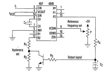
Comparison of an input signal's frequency (fi) with that of voltage-controlled oscillator (fVCO) can be accomplished with just one CMOS phase-locked loop IC and a transistor (see figure). The phase and the frequency can be compared with a phase comparator, which, along with the VCO, is part of the HEF4046 PLL IC. The transistor helps introduce hysteresis, enabling the circuit to be used as a switch driver. (View)
View full Circuit Diagram | Comments | Reading(2259)
Op amp application input end zeroing circuit diagram 1
Published:2011/5/16 21:52:00 Author:Rebekka | Keyword: Op amp application , input end zeroing
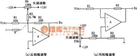
Figure (a) is a relatively simple circuit. It uses the input resistors R1 and the feedback resistor R2 as a part of the attenuation network. It generates a variable offset voltage with resistor R3 at the inverting input end. The voltage of the circuit is divided by R3 and R1,R2. The 2 ends of the potentiometer R4 connect with ± 15V power supply. The partial pressure ratio is about 1000 / 1. It can get ± 15mV offset voltage range. In figure (a), the general formula of the offset voltage adjustment range is:
Offset voltage range = ± VD · [(R1 ∥ R2) / R3] (± VD = ± 15V)
When there are multiple input signals at the reverse side. It is shown in figure (a) by the virtual display line. Its offset voltage range: Multiple input offset voltage range = ± VD [(R1 ∥ R2 ∥ Rl ') / R3] (± VD = ± l5V).
The circuit shown in figure (b) has a large application value. Since the adjusting voltage has no relationship with the feedback components, while the adjusting voltage is applied to the phase input terminal and avoid the winning stream signaling pathways. In this circuit, the resistance value of R3 and R5(100kΩ, 100Ω) form the 1000 / I voltage dividing circuit. The 2 terminals of R5 get ± 15mV offset voltage adjustment range. When the values of R3, R5 change. The offset voltage adjustment range is determined by:
Offset voltage adjustment range = ± VD · (R5/R3) (± VD = ± l5V) (View)
View full Circuit Diagram | Comments | Reading(500)
STEADY_TONE_INFRARED_TRANSMITTER
Published:2009/6/19 4:14:00 Author:May
This oscillator pulses an IR LED at about 1000 Hz. It should be useful as a test for lining up IR communications links or setting up fiber-optic cables, etc. (View)
View full Circuit Diagram | Comments | Reading(588)
IMD_TEST_CIRCUIT_FOR_PIN_DIODES
Published:2009/6/19 4:14:00 Author:May
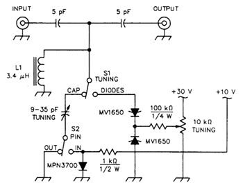
A loosely coupled tuned circuit for testing IMD production by PIN and tuning diodes in a narrow-band preselector, S1, TUNING, selects whether C1 or a pair of back-to-back MV1650 tuning diodes resonate L1. S2, PIN, adds or removes an MPN3700 PIN diode in series with C1. L1 consists of 33 turns of #28 enameled wire on a t-37-6 toroidal powdered-iron core. The MV1650, a 20-V tuning diode, exhibits a nominal capacitance of 100 pF at a tuning voltage of 4V. (View)
View full Circuit Diagram | Comments | Reading(891)
DOPPLER_ULTRASOUND_RECEIVER
Published:2009/6/19 4:13:00 Author:May
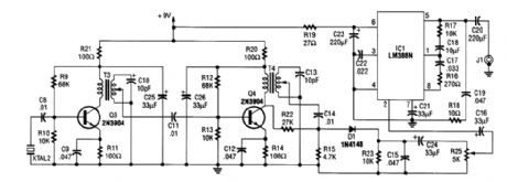
XTAL1 drives amplifjer Q3/Q4, which is tuned to 2.25 MHz. The detected signal is fed to audio amp!ifier IC1. A 9-V supply is used. The circuit operates at 2.25 MHz and is designed to be used with an ultrasonic sound transmitter at this frequency. (View)
View full Circuit Diagram | Comments | Reading(888)
IR_DETECTOR_CIRCUIT
Published:2009/6/19 4:13:00 Author:May
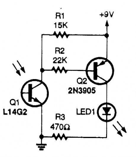
The circuit uses an IR phototransistor, Q1, to detect a remote control's IR output signal. A PNP transistor, Q2, then amplifies Q1's output and lights LED1. That indicates that an infrared signal has been detected by the phototransistor, or in other words, that your remote control works. (View)
View full Circuit Diagram | Comments | Reading(1732)
Photodiode isolation amplifier circuit diagram composed of ISO212P
Published:2011/6/26 22:06:00 Author:Rebekka | Keyword: Photodiode isolation , amplifier circuit
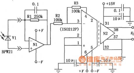
Photodiode isolation amplification circuit uses the photodiode to provide a reliable power supply isolation between the signal path and the two channels of the power supply. IS0212P is a low-cost miniaturized transformer-coupled isolation amplifier circuit. The chip uses two high-efficiency small toroidal transformer and provide reliable isolation between the signal path and the two channels of the power supply. Figure shows the typical application of IS0212P in optical detection, the photodiode is added to the two inputs of BPW21 and OPAl28 (N1) and forms the I / U resistor gain, it uses a larger feedback resistor. (View)
View full Circuit Diagram | Comments | Reading(1350)
INFRARED_BODY_HEAT_DETECTOR
Published:2009/6/19 4:12:00 Author:May
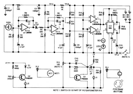
This circuit uses a pyroelectric detector to detect IR emissions in the 6- to 14-micron range. It is useful for security or infrared experiments. PYR1 is a pyroelectric IR detector. The unit should be mounted in a case with an IR lens to focus energy on the detector. (View)
View full Circuit Diagram | Comments | Reading(2235)
DOPPLER_ULTRASOUND_TRANSMITTER
Published:2009/6/19 4:12:00 Author:May

The 2.25-MHz oscillator Q1 drives amplifier Q2 and XTAL1, an ultrasonic transducer. The trans-ducer is a lead zirconate-titanate type. Taps on T1 and T2 provide low-impedance drive points. (View)
View full Circuit Diagram | Comments | Reading(1273)
LOW_POWER_INFRARED_DATA_LINK_RECEIVER
Published:2009/6/19 4:11:00 Author:May

The Maxim MAX403 in this circuit consumes only 1 mA and is capable of speeds over 1 MBPS. (View)
View full Circuit Diagram | Comments | Reading(736)
The offset zeroing circuit of differential amplifier
Published:2011/5/12 5:08:00 Author:Rebekka | Keyword: differential amplifier, offset zeroing

The offset zeroing circuit of differential amplifier is shown as above. When you lead the offset adjusting voltage to the differential amplifier circuit, it should not affect the balance of differential mode signal. In the circuit high-voltage divider ratio composed of R3 and R5. It provides variable potential to the right end of R2. Then it is passes R1 and R2 partial pressure. It gains the offset adjusting voltage at the inverting input of op amp. Generally the value of resistance R5 is small, its purpose is to raise partial pressure ratio. In order to obtain a high accuracy, sometimes in order to reduce the introduction of the common mode error, you need to adjust R2' to achieve the purpose.
R2/R1=(R2'+R5)/R1'
The circuit is shown in Fig. Its offset adjust voltage range determined by the following:Offset voltage range = VD (R5 / (R3 + R5)) (R1 '/ R1' + R2 ')Based on the data graph, the offset adjustment range is ± 15mV. (View)
View full Circuit Diagram | Comments | Reading(671)
IR_ILLUMINATOR_FOR_NIGHT_VISION_TV_CAMERAS_AND_SCOPES
Published:2009/6/19 4:10:00 Author:May

This Source uses LEDs and an astable oscillat to control the switch,duty-cycle,and effective IR illumination output. (View)
View full Circuit Diagram | Comments | Reading(1837)
567 FM demodulator
Published:2011/7/17 23:02:00 Author:zj | Keyword: FM demodulator

As shown in Figure it is 567 FM demodulation circuit. In the figue, the FM signalenters from the 3 foot, the demodulated signal goes out from 5 foot. FM signal center frequency which the circuit can demodulateis: fo = 1.1 / RC, C1 isfilter capacitor, and C2 is bandwidth adjustment capacitor. WhenC2 decreases, the demodulator demodulating bandwidth increases. The circuitalso hasdemodulation circuit. When the demodulation is correct, 8 footoutput level is low. The indicating lamp, indicator light, also can be removed and used as control signals. (View)
View full Circuit Diagram | Comments | Reading(2061)
| Pages:1398/2234 At 2013811382138313841385138613871388138913901391139213931394139513961397139813991400Under 20 |
Circuit Categories
power supply circuit
Amplifier Circuit
Basic Circuit
LED and Light Circuit
Sensor Circuit
Signal Processing
Electrical Equipment Circuit
Control Circuit
Remote Control Circuit
A/D-D/A Converter Circuit
Audio Circuit
Measuring and Test Circuit
Communication Circuit
Computer-Related Circuit
555 Circuit
Automotive Circuit
Repairing Circuit