
Circuit Diagram
Index 1401
Z_DICE_GAME
Published:2009/6/19 3:38:00 Author:May


Using a microcontroller (U2) keeps the parts count and the cost of this 5-dice LED display relatively low. Z-dice uses five clusters of seven LEDs to represent the marks or pips on five dice. Buttons below each of the LED dice let the player mark a die to be rolled on the next throw. Marked dice show up as dimmed LEDs. Pressing the button to the right of the display rolls the marked dice. If the player changes his or her mind about rolling a particular die before pressing the roll button, he or she can un-mark it by pressing its button a second time. If no dice are marked at the time the player presses the roll button, then all of the dice are marked to be rolled. A second press starts them rolling, animating the LEDs of the marked dice for a second or so before displaying the results of the roll. Z-Dice doesn't count rolls or keep score, so it's still up to the players to make sure that nobody cheats!This diagram shows the wiring details of the dice display. For space and simplicity, only the first and last dice are shown. A programmed microcontroller is needed for this circuit. Refer to the original article for software. (View)
View full Circuit Diagram | Comments | Reading(1191)
Self-initiated control overcurrent protection circuit diagram
Published:2011/6/24 1:43:00 Author:Rebekka | Keyword: Self-initiated control , overcurrent protection

If the RS flip-flop reset still in the over-current condition, the level of FF1's Q-side is always high. It continues to cut off the device power supply. IC1 has been in the set state. The R side of FF1 does not work. The control circuit of the overcurrent devices can not only cut off the power and when it returns to be normal, it can start automatically. Thus the power interruption error which is generated by the phenomenon can be removed. (View)
View full Circuit Diagram | Comments | Reading(502)
FIRST_RESPONSE_MONITOR_I
Published:2009/6/19 3:33:00 Author:May
Three interlocked flip-flops enable the detection of the first input. S1, S2, and S3 are inputs.Analog switches controlled by logic gates, or other logic circuitry could be sub-statement for S1, S2, and S3. (View)
View full Circuit Diagram | Comments | Reading(599)
FURNACE_FUEL_MISER
Published:2009/6/19 3:33:00 Author:May

A timer (LM555CN) and decode counter is used to generate duty cycles from 10% to 100% to control the time a heating system can operate. V2 is a decode counter that can be switched from 10% to 100% duty cycle. V3A and B form a latch that drive A1, LED1, and V4. The triac TRI is used as an ac switch, in series with the thermostat that controls the heating system. (View)
View full Circuit Diagram | Comments | Reading(788)
Multi-purpose household protection circuit composed of the C036
Published:2011/6/24 3:23:00 Author:Rebekka | Keyword: Multi-purpose household protection

Delayed protection circuit is mainly composed of the charge and discharge loop (R6, C5), YF1 and the RS flip-flop, relay J3, driver circuit (BG2, BG3) composed of YF2. When it is connected with the power supply, because the voltage on C5 is not mutation, YF1 outputs low. It makes BG2, BG3 conducted, the relay J3 will be pulled in. The load starts to work because the J3-1 is connected to the power supply. (View)
View full Circuit Diagram | Comments | Reading(617)
NOVEL_RF_POWER_METER
Published:2009/6/19 3:32:00 Author:May
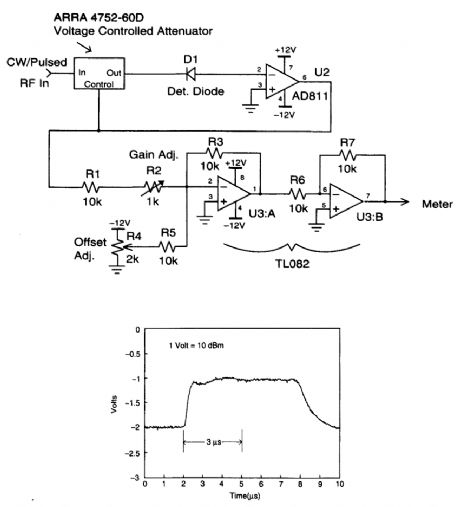
The circuit matches the diode with a voltage-variable attenuator that has a logarithmic response. By varying the attenuation until the diode output is zero, the resulting attenuation value then corre-sponds to the input power level. Because the voltage-variable attenuator's output is logarithmic, diode nonlinearities become negligible. (View)
View full Circuit Diagram | Comments | Reading(668)
TWO_REMOTE_METERS
Published:2009/6/19 3:29:00 Author:May
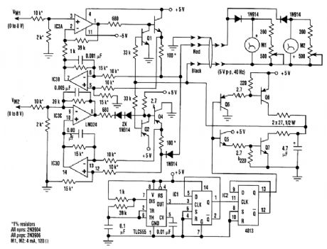
Two remote meters can be driven independently using just one wire pair. This“constant current”design eliminates the effects of wire-pair resistance up to 200Ω. Driving two remote meters inde-pendently usually requires two wire pairs(one pair for each meter).In the circuit, IC1 and IC2 generate a 40-Hz symmetrical square wave (the frequency isn't criti-cal). Q5 through Q8 amplify tl)e square wave to 5 Vp-p, which is applied to the return (black wire)for the remote meters.Amplifier IC3A buffers the input signal voltage Vmi, intended for meter M1(0 to 8V), and sends it through emitter-follower Q3 to a 100-Q current-sense resistor. The other end of this resistor is tied to the supply (red wire) of the remote meters. IC3B amplifies the voltage across the sense resistor, which corresponds to the current sent to remote meter MI, and closes the feedback loop to IC3A.This results in a voltage of 0 to 8V at the Ml input, generating a current of 0 to 10 mA to M1.Transistor Q1 gates this current on and off synchronous to the 40-Hz square wave so that meter MI actually sees a 50% 0-to-+10-mA peak(0 to 5 mA average)current.Similarly, IC3C, IC3D, Q2, and Q4 provide a 0- to -10-mA peak current for M2. Ml and M2 are isolated by the two-reverse-conn ected 1N914 diodes in the remote-meter box. Variable resistors across Ml and M2 permit calibration. The extra 1N914 diode in the M2 drive circuit prevents inter-ference between MI and M2. (View)
View full Circuit Diagram | Comments | Reading(521)
SOLDERING_IRON_CONTROL
Published:2009/6/19 3:28:00 Author:May

A current control to temperature regulate a soldering iron uses a high-voltage integrated reg-ulator, TL783 (U1). Wlth the component values specified, the circuit should be used with a sol-dering iron of 25 W or less. (View)
View full Circuit Diagram | Comments | Reading(2602)
Temperature range controller circuit diagram composed of 555
Published:2011/6/27 5:06:00 Author:Rebekka | Keyword: Temperature range controller

When the temperature falls below the lower temperature, the resistance R1 becomes larger, so that 555 ② feet is lower than the potential 1/3Vcc. The corresponding 555 sets, ③ pin outputs high level. The light-emitting diode LED2 is lit, the relay J1 is pulled in. Connect J1-3 to the heater power supply to heat. When the temperature reaches the maximum temperature. The R1 resistance becomes smaller. The potential of 555 ⑥ will be greater than feet 2/3Vcc. The ② the foot of the potential must be greater than 1/3Vcc, reset the corresponding 555, ③ pin outputs low level. The light-emitting diodes LED1 is lit, the relay J1 releases, the contact J1-3 is disconnected. (View)
View full Circuit Diagram | Comments | Reading(1275)
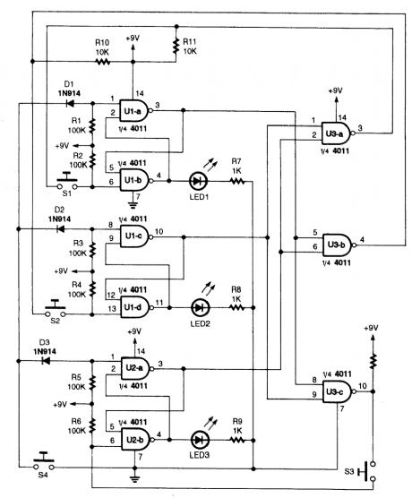
ELECTRONIC_CRAPS_GAME
Published:2009/6/19 3:26:00 Author:May

Two gates of a 4093 quad, 2-input NAND, Schrnitt-trigger CMOS IC are connected in astable-os-cillator circuits as clocks. The two 4017ICs have six LEDs connected to its first six outputs. As the clock pulses enter pin 14 of the 4017s, the ICs count from one to six over and over as long as the clock pulses are present. When S1 and/or S2 are released, one of the LEDs in each circuit will remain on, indicating a number from one to six.The circuit is set up so that you can roll the dice together by pressing S1 and S2 at the same time, or roll each die one at a time. (View)
View full Circuit Diagram | Comments | Reading(2270)
Variable gain differential amplifier circuit composed of the μA709
Published:2011/6/27 5:14:00 Author:Rebekka | Keyword: Variable gain, differential amplifier
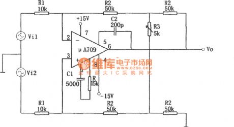
The figure shows variable gain differential amplifier circuit composed of the μA709. The biggest advantage of this circuit is to maintain common-mode rejection and keep the ratio KCMR in the same premise. The differential gain can be achieved continuously adjustable. The biggest advantage of this circuit is to maintain common-mode rejection ratio KCMR the same premise, the differential gain can be achieved continuously adjustable. The circuit of the basic relationship is: Vo =- (2R2/R1) · (1 + R2/R3) · (Vi1-Vi2) Av = Vo / (Vi1 a Vi2) =- (2R2/R1) · (1 + R2 / R3) When R1 = 10kΩ, R2 = 50kΩ, R3 = 5kΩ when, Av =- 110. μA709 integrated chip electrical parameters (VD = ± 15V, TA = 25 ℃). (View)
View full Circuit Diagram | Comments | Reading(1626)
WIDE_RANGE_FUNCTION_GENERATOR
Published:2009/6/19 3:24:00 Author:May
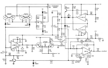
The sine, square, triangle function generator is exceptionally useful. Various IC circuits have been published for generating square and triangle waveforms in an attempt to duplicate the general-purpose function generator. However, these simple circuits are usually limited to about 10 kHz and have no sine-wave output. The function generator shown here provides all three waveforms and operates from below 10 Hz to 1 MHz with usable output to about 2 MHz. (View)
View full Circuit Diagram | Comments | Reading(2591)
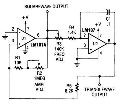
ACCURATE,STABLE_FUNCTION_GENERATOR
Published:2009/6/19 3:21:00 Author:May

Supply-limited oscillators usually are sensitive to temperature and power-supply changes, are never symmetrical, and don't operate at high frequencies because the amplifier's output is saturated when it reaches the supply lines.The circuit shown, a function generator, can alleviate these problems. Its square-wave output boasts a rapid rise time, quick settling time, and an amplitude that's temperature insensitive. Also, its triangular output waveform features a perfectly constant rate of change throughout its range.Amplifier A1 together with A2 generates a stable +10 V. This signal, which is integrated using A3, C2, and R2, makes a negative-going ramp. When the peak output of A3 equals -10 V, the output of A1 and A2 change state and the A3's output ramps up. When A3's output equals +10 V, the outputs of A1 and A2 change state again and new cycle starts. (View)
View full Circuit Diagram | Comments | Reading(816)
VOICE_DISGUISER
Published:2009/6/19 3:20:00 Author:May

A complete schematic diagram of the voice disguiser is shown. Microphone MIC1 picks up the voice signal and feeds it to an audio amplifier, consisting of Q1 and Q2, and a few support compo-nents. The amplifier has a low-pass gain response that limits the voice frequencies to 5 kHz or lower.
The voice signal is then fed to the input of the first balanced modulator, which is comprised of U1-a, U1-b, U2-a, and U3-a. The output of the first 4-kHz oscillator, built around U3-f and U3-e, is fed to the carrier input of the first modulator. The frequency of the first oscillator is controlled by the setting of potentiometer R13. The modulator output-a double-sideband suppressed-carrier signal centered on 4 kHz-is then filtered by the first 5-kHz low-pass filter, formed by U2-b, which elimi-nates the upper-sideband signals.
At this point, the voice frequency spectrum is inverted (e.g., the frequencies that were low now become high, and vice versa), making the voice signal completely unintelligible. The output of the first low-pass filter is fed to a second modulator formed by U1-c, U1-d, and U3-b, where it is fre-quericy modulated with the output of the second carrier oscillator, comprised of U3-c and U3-d; the frequency of the second oscillator is controlled by potentiometer R36.
The output of the second modulator is filtered by the second low-pass filter, which consists of U2-d and few support components, and amplified by Q3. The voice output signal from Q3 is fed to U4 (an LM386 low-voltage, audio-power amplifier) through an impedance-matching transformer, T1.The output of U4 is then used to drive SPKR1 (an 8-Ω speaker).
In operation, if both carrier oscillators are set to the same frequency, the voice signal from the speaker will be an exact duplicate of the input signal from the microphone. However, if the frequency of the second oscillator is varied (via R36), the output voice signal also shifts in frequency. That makes the voice reproduced by the speaker sound higher- or lower-pitched than normal. (View)
View full Circuit Diagram | Comments | Reading(1272)
SIMPLE_FUNCTION_GENERATOR
Published:2009/6/19 3:18:00 Author:May
View full Circuit Diagram | Comments | Reading(671)
SWEEP_FUNCTION_GENERATOR_1
Published:2009/6/19 3:17:00 Author:May


Both IC2 and IC4 are Exar XR2206 monolithic function generators; IC4 functions as a ramp gen-erator, and IC2 functions as a generator of sine, triangular, and square waveforms. Dual operational amplifier IC1 produces a scaled, level-shifted ramp output that is capable of deflecting an oscillo-scope's horizontal sweep.Any frequency of interest along the horizontal axis of an oscilloscope that is coupled to this func-tion generator can be mgasured with an external frequency counter by manually tuning the function generator's VCO instead of sweeping it. The performance characteristics of the sweep/function gen-erator are summarized in the Table.The generator's sweep rate and frequency can be set by front-panel rotary six-position switches, Sweep Rate Switch S5 and Frequency Switch S2. The VCO control R30 manually tunes the VCO.Table 2 lists the sweep ranges of the function generator. Sweep ranges not covered in ranges 1 to 4 can be set up as required on positions 5 and 6. Selecting the VCO setting on the front panel toggle switch S4 permits tuning any fixed frequency within the total frequency range of the instrument with both frequency switch S2 and VCO control R30.The sweep rate or duration of the sweep ramp is selected by the rotary six-position Sweep Rate Switch S5. Table 3 lists the sweep rate durations for each of the six positions. Longer periods should be used for lower frequency sweeps. (View)
View full Circuit Diagram | Comments | Reading(4267)
GATE_DIP_OSCILLATOR_II
Published:2009/6/19 3:17:00 Author:May

Useful for measuring the resonant frequencies of antennas, tuned circuits, and also as a tuned detector, this circuit is a modem variation of the classic vacuum tube grid dip oscillator. It coupled the G.D.O. to a tuned circuit and caused RF energy to be absorbed by the unknown tuned ctrcutt when the G.D.O. frequency was the same as that of the tuned circuit in question. This showed as a dip in the meter reading. (View)
View full Circuit Diagram | Comments | Reading(2604)
NICAD_BATTERY_CHARGER_1
Published:2009/6/19 3:13:00 Author:May

This circuit has a current regulator and uses an external timer to control the charging rate. (View)
View full Circuit Diagram | Comments | Reading(1118)
LEAD_ACID_TRIOKLE_CHARGER
Published:2009/6/19 3:10:00 Author:May

This lead-acid battery trickle charger can be used as a stand-alone circuit (for alarm systems and such) or combined with the circuit in the figure to create an emergency lighting system. (View)
View full Circuit Diagram | Comments | Reading(1145)
Breeze ceiling fan temperature controller circuit composed of the NE555
Published:2011/6/28 3:16:00 Author:Rebekka | Keyword: Breeze ceiling fan, temperature controller

When environment temperature increases, the resistance of the corresponding R7 R6 become smaller and make the IC (2) feet down to less than a third potential VDD and it is reset, 3 feet output high level. So the controlled silicon AC zero-voltage switching composed of D2~D5、SCR、BG1、BG2 will be turned on. Fan D operates when supply power is open; When the environment temperature falls, resistance of the corresponding R7, R6 changes, 555 is reset because the feet (2) is larger than a third potential VDD, (3) feet outputs low level, so that the controlled silicon AC zero-voltage switching is closed. The electric fan D stops because the power supply is closed. (View)
View full Circuit Diagram | Comments | Reading(997)
| Pages:1401/2234 At 2014011402140314041405140614071408140914101411141214131414141514161417141814191420Under 20 |
Circuit Categories
power supply circuit
Amplifier Circuit
Basic Circuit
LED and Light Circuit
Sensor Circuit
Signal Processing
Electrical Equipment Circuit
Control Circuit
Remote Control Circuit
A/D-D/A Converter Circuit
Audio Circuit
Measuring and Test Circuit
Communication Circuit
Computer-Related Circuit
555 Circuit
Automotive Circuit
Repairing Circuit