
Circuit Diagram
Index 1405
DUAL_CONTROL_HEXFET_SWITCH
Published:2009/6/19 2:33:00 Author:May

This dual-control switch uses two 6 to 10-Vac sources to trigger the circuit on and off; one source for each function. (View)
View full Circuit Diagram | Comments | Reading(587)
555 micro defibrillation emergency device circuit
Published:2011/5/2 22:51:00 Author:May | Keyword: 555, micro, defibrillation, emergency device
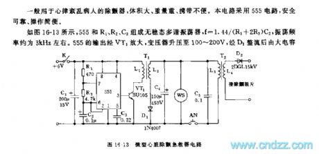
The defibrillator ordinary used for arrhythmia patient is bulky, heavy and inconvenient to carry. This circuit adopts 555 circuit, it is safe and reliable, and the operation is simple.
As shown in diagram 16-13, astable multivibrator consists of 555 and R1, R2, c2, f=1.44/(R1+2R2)C2, its oscillation frequency is about 3kHz. Output of 555 is enlarged by VT1, transformer can set up to 100~200V, it is rectified by D1 and stored energy by big capacitor C3. When using and pressing AN, C4 discharges by the primary stage L3 of T2, and the secondary stage L4 is induced high voltage 1000~7000V and defibrillation for arrhythmia patient.
(View)
View full Circuit Diagram | Comments | Reading(2783)
1_kHz_4TH_ORDER_BUTTERWORTH_FILTER
Published:2009/6/19 2:33:00 Author:May


The filter is a simplified state variable architecture consisting of two cascaded 2nd-order sections. Each section uses the 360° phase shift around the two op-amp loop to create a negative sum-ming junction at Al's positive input. The circuit has low sensitivities for center frequency and Q, which are set with the following equations:where,The dc bias applied to A2 and A4, half supply, is not needed when split supplies are available.The circuit swings rail-to-rail in the passband making it an excellent anti-aliasing filter for A/Ds. The amplitude response is flat to 1 kHz then rolls off at 80 dB/decade. (View)
View full Circuit Diagram | Comments | Reading(1087)
ELECTROSCOPE
Published:2009/6/19 2:32:00 Author:May
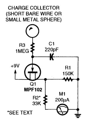
This circuit is useful for detecting electrostatic charges. In operation, C1 reduces ac noise, but lowers the sensitivity a bit. The MPF102 and R1 form a voltage divider. When the FET's gate is earth-grounded, the divider's output will be about 4.5 V giving a half-scale reading on Ml, a 200-μA meter. A positively charged object(like cotton-rubbed glass)will give a positive deflection from half-scale, and a negatively charged object (a plastic comb, for ex-ample)will give a negative meter deflection.The whole circuit(including the 9-V battery supply)should be in a metal enclosure, and a short piece of bare wire makes a fine charge collector. (View)
View full Circuit Diagram | Comments | Reading(3)
555 electronic storage device
Published:2011/5/2 22:54:00 Author:May | Keyword: 555, electronic, storage device
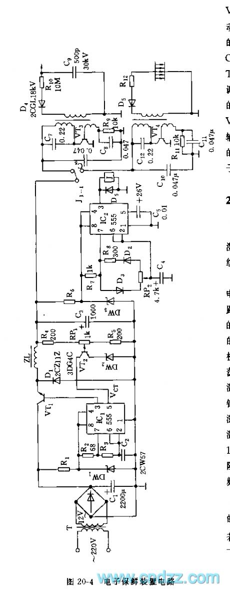
As shown in diagram 20-4, electronic storage device consists of constant voltage source, oscillator, negative-ion generator and ozone generator.
Constant voltage source adopts 555 and R2, R3, C2, etc to make up astable multivibrator, VT1 is switching regulating pipe, R4, RP1, R5 and VT2, etc make up sampling amplifier, it controls pin 5 of IC1, it can automaticly adjust 555's output pulse duty factor, thereby it can achieve the purpose of voltage regulation. D1 is fly-wheel diode. IC2 and R7, R8, RP2, C4, etc make up duty factor adjustable multivibrator type oscillator, oscillation period T=0.693(R7+R8+RP2)C4. The feature of this circuit is: when RP2 is adjusted, it not changes its oscillation frequency and only changes the duty factor of waveform. When pin 3’s output is high level, J pulls in, it makes negative-ion generator composed of VT4, etc to energized and worked. When output of 555 is low level, J is released, J1-1 is connected power supply of ozone generator, it can make the two work in turns, the released ozone and negative-ion can keep vegetables and fruits fresh. (View)
View full Circuit Diagram | Comments | Reading(1185)
CAPACITOR_DISCHARGE_IGNITION_SYSTEM
Published:2009/6/19 2:31:00 Author:May


This ignition system charges a capacitor (C2) to 350 V and discharges it through the ignition coil. (View)
View full Circuit Diagram | Comments | Reading(1529)
RC_NOTCH_FILTER
Published:2009/6/19 2:31:00 Author:May

View full Circuit Diagram | Comments | Reading(688)
ACTIVE_HIGH_PASS_FILTER
Published:2009/6/19 2:30:00 Author:May

View full Circuit Diagram | Comments | Reading(0)
SALLEN_KEY_LOW_PASS_FILTER
Published:2009/6/19 2:30:00 Author:May

View full Circuit Diagram | Comments | Reading(633)
74 series digital circuit 74LS465/466 etc eight bus buffer (three state)
Published:2011/5/13 5:10:00 Author:May | Keyword: digital, eight bus buffer, three state

74LS465 is in-phase gatepermiting input, 74LS466 is opposite phase gate controlpermiting input,74LS467 is in-phase four lines and four linespermiting input. The function and pin diagram of 74LS465~468 is seperately same to 74LS795~798. (View)
View full Circuit Diagram | Comments | Reading(813)
BANDPASS_FILTER
Published:2009/6/19 2:29:00 Author:May

View full Circuit Diagram | Comments | Reading(0)
HIGH_POWER_12_V_IC_AUTO_AMPLIFIER
Published:2009/6/19 2:29:00 Author:May

View full Circuit Diagram | Comments | Reading(697)
20_kHz_BUTTERWORTH_ACTIVE_FILTER
Published:2009/6/19 2:29:00 Author:May

This filter will be useful for anti-aliasing or band limiting in an audio system.The op amp is a Linear Technology, LT1124,LT1355,or LT1169. (View)
View full Circuit Diagram | Comments | Reading(808)
Small non-contact refrigerator time delay protector circuit diagram
Published:2011/5/15 6:03:00 Author:Rebekka | Keyword: Small non-contact refrigerator, time delay protector

The protector circuit is shown in the figure 1. 220V AC power passes the capacitor C1 buck, VD1 half-wave rectifier to the regulated VDW the time base circuit 555 as a working power supply. When it connects to power supply for about 5 minutes, the time base circuit ③ foot outputs from low to a high level. The two-way thyristor VS will be conducted to work and provides power supply for the refrigerator. At this time the light-emitting diode LED is lit. It indicates the power supply is normal. (View)
View full Circuit Diagram | Comments | Reading(2511)
74 series digital circuit 74LS386 and other four two input XOR gate
Published:2011/5/13 5:09:00 Author:May | Keyword: digital, four two input, XOR gate


View full Circuit Diagram | Comments | Reading(931)
HIGH_POWER_AUDIO_AMP_FOR_AUTOMOTIVE_INSTALLATION
Published:2009/6/19 2:29:00 Author:May

Two of these audio amplifiers can be used to make a stereo amplifier 200W per channel. IRF640 and IRF9640 power MOSFETs are used to drive the output load, which might be 4 or 8Ω. Response is 12 Hz to 45 kHz (-3 dB), THD <0.1%. Power is supplied by a switching-type power supply, which is external to the amplifier (±47V). About 600 W total power (peak) is needed. (View)
View full Circuit Diagram | Comments | Reading(8023)
74 series digital circuit 74LS379 eight D flip flop
Published:2011/5/13 5:08:00 Author:May | Keyword: digital, eight, D flip flop

74LS379, 74F379, 74S379, 74HC379 eight D flip flop74××175 is similar to this circuit. It only has one common allow end, and not common clear end.function table ( every flip flop)Q0=the level of Q before building stable state input condition
(View)
View full Circuit Diagram | Comments | Reading(1558)
74 series digital circuit 74LS378 74F378 and other six D flip-flop
Published:2011/5/13 5:08:00 Author:May | Keyword: digital, six D flip-flop

74LS378, 74F378, 74S378, 74HC378 six D trigger74××174 is similar to this circuit. It only has one public permitting but not public clearing end. (View)
View full Circuit Diagram | Comments | Reading(721)
REMOTE_TWO_WAY_ac_SWITCH_HOOkUP
Published:2009/6/19 2:28:00 Author:May

This switching arrangement is the type of arrangement used in both domestic and industrial environments to allow a light or other ac-operated device to be controlled from more than one location (View)
View full Circuit Diagram | Comments | Reading(567)
74 series digital circuit 74LS377 and other eight D flip-flop
Published:2011/5/13 5:06:00 Author:May | Keyword: digital, eight D flip-flop


Q0=the level of Q before building stability input condition.74LS377, 74F377, 74S377, 74HC377 eight D trigger74××273 is similar to this circuit. It only has one public permitting but not public clearing end. (View)
View full Circuit Diagram | Comments | Reading(746)
| Pages:1405/2234 At 2014011402140314041405140614071408140914101411141214131414141514161417141814191420Under 20 |
Circuit Categories
power supply circuit
Amplifier Circuit
Basic Circuit
LED and Light Circuit
Sensor Circuit
Signal Processing
Electrical Equipment Circuit
Control Circuit
Remote Control Circuit
A/D-D/A Converter Circuit
Audio Circuit
Measuring and Test Circuit
Communication Circuit
Computer-Related Circuit
555 Circuit
Automotive Circuit
Repairing Circuit