
Circuit Diagram
Index 1411
SIMPLE_HIGH_GAIN_AUDIO_AMPLIFIER
Published:2009/6/18 23:53:00 Author:May
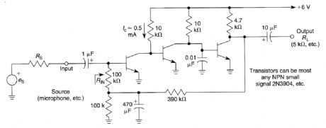
This amplifier has a very high gain in the audio range and is approximately the product of the current gains of the three transistors multiplied by the ratio of RL to (RIN+RS).RIN is approximately to: (View)
View full Circuit Diagram | Comments | Reading(894)
FET_PHONO_CARTRIDGE_PREAMP
Published:2009/6/18 23:51:00 Author:May
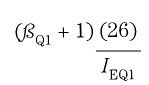
A high-Z phono cartridge can be rnatched to a low-Z amplifier with this circuit. The FET provides a current gain of over 1000x and a voltage gain of about 0.5x. (View)
View full Circuit Diagram | Comments | Reading(690)
STEREO_TV_DECODER
Published:2009/6/18 23:51:00 Author:May


A block diagram of the stereo-TV decoder is shown in A. It shows the overall relationships be-tween the separate sections of the circuit; B through E show the details of each subsection. The de-coder section centers around IC1, a standard 4.5-MHz audio demodulator. The output of IC1 is routed to 51, which allows you to choose between the internally demodulated signal and an exter-nally demodulated one. Buffer amplifier IC2-a then provides a low-impedance source to drive IC3, an LM1800 stereo demodulator.When IC3 is locked on a stereo signal, the outputs presented at pins 4 and 5 are discrete left- and right-channel signals, respectively. In order to provide noise reduction to the L-R signal, you must recombine the discrete outputs into sum and difference signals. Op amp IC4-a is used to regenerate the L-R signal. It is wired as a difference amplifier, wherein the inputs are summed together (+L -,R). Capacitor C18 bridges the left- and right-channel outputs of the demodulator. Although it decreases high-frequency separation slightly, it also reduces high-frequency distortion.The L + R signal is taken from the LM1800 at pin 2, where it appears at the output of an internal buffer amplifier. The rawL -R signal is applied to IC4-b, a 12-kHz lowpass filter. The L + R signal is also fed through a 12-kHz low pass filter in order to keep the phase shift undergone by both signals equal.Next, the L - R signal is fed to Q2. It allows you to add a level control to the L - R signal path; it provides a low source impedance for driving the following circuits, and it inverts the signal 180°. In-version is necessary to compensate for the 180°inversion in the compander.Next comes the expander stage. At the collector of Q2 is a 75-μs de-emphasis network (R27 and C29) that functions just like the network that is associated with Q1. Note that Q2 feeds both Q3 and IC5-a, a -12-dB per octave high-pass filter. The output of that filter drives the rectifier input of IC6, an NE570. The 75-Hz high-pass filter at the rectifier input helps to prevent hum, 60-Hz sych buzz, and other low-frequency noise in the L - R signal from causing pumping or breathing.The NE570 contains an on-board op amp; its irtverting input is available directly at pin 5 and via a 20-kO series resistor at pin 6. The 18-kQ resistor (R30) combines with the internal resistor and C32 (0.01 μF) to form a first-order filter with a 390-μs time constant. Because the internal op amp oper-ates in the inverting mode, the -(L - R) signal is restored to the proper (L - R) form.The output of the expander drives another 75-Hz high-pass filter, but this one is a third-order type that provides -18 dB per octave rolloff. It is used to keep low-frequency noise from showing up at the output of the decoder. At this point, the (L - R) signal has been restored, more or less, to the condition it was in before it was dBx companded at the transmitter. (View)
View full Circuit Diagram | Comments | Reading(291)
HIGH_GAIN_DYNAMIC_MICROPHONE_PREAMPLIFIER
Published:2009/6/18 23:50:00 Author:May
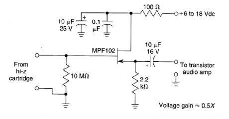
This microphone preamplifier is capable of about 70 dB or more gain at audio frequencies. Its gain is approximately equal to the product of the hfe of both transistors times the ratio of the load resistance to the input resistance of the preamp. As an approximation, these resistances are usually similar in value (≈2 to 5 kΩ) for most applications, so this ratio can be taken as unity. (View)
View full Circuit Diagram | Comments | Reading(1381)
SIMPLE_20_dB_GAIN_AUDIO_AMPLIFIER
Published:2009/6/18 23:49:00 Author:May
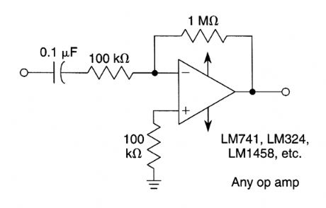
View full Circuit Diagram | Comments | Reading(1285)
LOW_LEVEL_AUDIO_AMPLIFIER
Published:2009/6/18 23:48:00 Author:May

View full Circuit Diagram | Comments | Reading(660)
SINGLE_ENDED_HI_Z_MICROPHONE_PREAMP
Published:2009/6/18 23:47:00 Author:May

This low noise circuit works on a +5-V supply. Gain range is 20 to 40 dB and bandwidth is 20 kHz with the AD820. THD is 0.05% with 1 V RMS into a 2-kΩ load. Noise output with the input shorted is less than 200μV. (View)
View full Circuit Diagram | Comments | Reading(1247)
LOGIC_CHIP_TESTER
Published:2009/6/18 23:46:00 Author:May

This device compares two logic signals and indicates whether the two logic signals are the same or different. To use the tester, first connect the test input to the suspect pin of the DUT. Next, con-nect the reference input to the same pin of an identical reference chip that is known to be good. Push the reset button to begin the test; the green section of the bicolor LED will be illuminated. Any sig-nal on the test device that differs from the one on the reference device will then mornentarily light the LED lamp that corresponds to that pin, and also latch on the red section of the bi-color LED. That indicates that the device under test is faulty. If the reference and DUT signals are the same, the DUT is OK, and the green LED will remain lit. (View)
View full Circuit Diagram | Comments | Reading(1064)
Beijing Hyundai Sonata motor-driven door and window switch circuit diagram
Published:2011/5/6 3:41:00 Author:muriel | Keyword: Beijing Hyundai Sonata, motor-driven, door and window, switch

Beijing Hyundai Sonata motor-driven door and window switch circuit diagram is as shown
(View)
View full Circuit Diagram | Comments | Reading(852)
0V to 12V adjustable regulated voltage circuit
Published:2011/3/30 2:13:00 Author:muriel | Keyword: 0V to 12V, adjustable, regulated voltage

View full Circuit Diagram | Comments | Reading(525)
0.6-1.5V/2-6A regulated voltage circuit
Published:2011/5/5 3:03:00 Author:muriel | Keyword: 0.6-1.5V/2-6A, regulated voltage circuit

When it uses the auxiliary power supply Uh, Itcanregulate output voltage low to U2 = 0.6 V(FIG. A). After Adjusted the potentiometer R8, itcan changethe load current of limitation whichmakes transistor loss powerless than its maximum allowable (FIG. B). The circuit of the main technical data:Technology data of the circuit: output voltage:U2=0.6V~15V output current:I2=2A~4A input voltage:U1=20.5V~30.8V internal resistance:Rg=40mΩ T1Radiator thermal resistance:Rthk≤0.64grd/W T2Radiator thermal resistance:Rthk≤10grd/W when ambient temperatureθu=0°C~60°C output voltage variable quantity: ΔU2=28mV when output current I2=0~4A(U1=constant,U2=15V), ΔU2=160mV input voltage U1=20.5~30.8V (View)
View full Circuit Diagram | Comments | Reading(542)
RIAA_LINE_AMPLIFIER_DRIVER
Published:2009/6/18 23:45:00 Author:May

Two op amps by Analog Devices are used in this audio Iine amplifier, which is suitable for interfacing with an RIAA preamplifier. (View)
View full Circuit Diagram | Comments | Reading(705)
BALANCED_MICROPHONE_PREAMPLIFIER
Published:2009/6/18 23:44:00 Author:May

A balanced input for microphones can solve hum and noise pickup problems. R6 and R13 should equal R5 and R12, respectively. Typical values would be 10 kΩ to 22 kΩ. (View)
View full Circuit Diagram | Comments | Reading(7033)
FM_STEREO_TRANSMITTER
Published:2009/6/18 23:44:00 Author:May

A BA1404 IC is used to generate a complete FM MPX signal. The chip contains all of the necessary circuitry. C1 and R3, and R4 and C4 provide pre-emphasis. The transmitter runs on a single AA cell. L3 is 3 tums of #20 wire on a 3/6 drill (for a form). L3 is1/4 long. L4 is 4 turns #20 wire on 3/6 drill bit, spaced to 3/8 . If monophonic operation is wanted, omit C5 and the 38-kHz oscillator components. (View)
View full Circuit Diagram | Comments | Reading(312)
DYNAMIC_MICROPHONE_PREAMP
Published:2009/6/18 23:43:00 Author:May

This preamplifier provides 40- to 43-dB gain when used with a low-impedance (<1kΩ) dynamic microphone (View)
View full Circuit Diagram | Comments | Reading(3)
TRANSISTOR_RIAA_PREAMP_FOR_MAGNETIC_PHONE_CARTRIDGES
Published:2009/6/18 23:42:00 Author:May
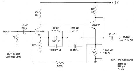
This two-transistor circuit has around 40 dB (midband) gain at 1 kHz. A magnetic cartridge is used as a source. (View)
View full Circuit Diagram | Comments | Reading(1597)
DUAL_CLOCK_CIRCUIT_FOR_STEPPER_MOTORS
Published:2009/6/18 23:41:00 Author:May

This oscillator can be used to drive a stepper motor circuit at two preset speeds with override to shut the motors off. (View)
View full Circuit Diagram | Comments | Reading(760)
PERSONAL_STEREO_AUDIO_AMP
Published:2009/6/18 23:40:00 Author:May
You can make your personal stereo do double duty as a small room stereo by adding this 2-watt amplifier. (View)
View full Circuit Diagram | Comments | Reading(689)
STEPPER_MOTOR_CIRCUIT_WITH_FET_DRIVERS
Published:2009/6/18 23:40:00 Author:May

This motor-driver circuit replaces the eight bipolar transistors of the previous circuit with four IFR511 power hexFET's (Q1 through Q4). (View)
View full Circuit Diagram | Comments | Reading(1643)
1_kW_POWER_METER
Published:2009/6/18 23:40:00 Author:May
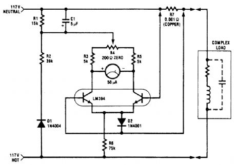
The power meter shown uses only one transistor pair to provide the complete (X)(Y)function.The circuit is intended for 117 Vac±50 Vac operation, but can be easily modified for higher or lower voltages. It measures true (nonreactive)power being delivered to the load and requires no external power supply. Idling power drain is only 0.5W. The load current-sensing voltage is only 10 mV, keep-ing load voltage loss to 0.01%. Rejection of reactive load currents is better than 100:1 for linear loads.Nonlinearity is about 1% full scale when using a 50-μA meter movement. The temperature correction for gain is accomplished by using a copper shunt (+0.32%/℃) for load-current sensing. This circuit measures power on negative cycles only, so it cannot be used on rectifying loads. (View)
View full Circuit Diagram | Comments | Reading(1495)
| Pages:1411/2234 At 2014011402140314041405140614071408140914101411141214131414141514161417141814191420Under 20 |
Circuit Categories
power supply circuit
Amplifier Circuit
Basic Circuit
LED and Light Circuit
Sensor Circuit
Signal Processing
Electrical Equipment Circuit
Control Circuit
Remote Control Circuit
A/D-D/A Converter Circuit
Audio Circuit
Measuring and Test Circuit
Communication Circuit
Computer-Related Circuit
555 Circuit
Automotive Circuit
Repairing Circuit