
Circuit Diagram
Index 1393
12_V_HIGH_VOLTAGE_SUPPLY_FOR_HE_NE_LASER
Published:2009/6/22 22:25:00 Author:May

T1 is a 6-V:330-V dc/dc inverter transforlrter with a 57.4:1 turn ratio, rated at 7W.R1 270-Ω resistorR2 180-kΩ resistor, 3 to 5 W C1 22-μF electrolytic capacitorC2 1-μF electrolytic capacitorC3-C6 0.02-μF capacitor,1 kV or moreD1 1N4001 diodeD2-D5 High-voltage diode(3 kV or more)Q1 TIP 140 power transistor T1 High-voltage dc-to-dc converter transformer; see text for speciftcattons
All resistors are 5 to 10% tolerance, 1/4 W, unless otherwise indicated. All capacitors are 10 to 20% tolerance, rated 35 V or more, unless otherwise indicated. (View)
View full Circuit Diagram | Comments | Reading(2292)
SIMPLE_TELEPHONE_RING_INDICATORLINE
Published:2009/6/22 22:25:00 Author:May

A neon lamp can easily be added to the phone line to act as a ring indicator. It's perfect for times when you can't hear the phone. (View)
View full Circuit Diagram | Comments | Reading(629)
BATTERY_CHARGER_PROBE
Published:2009/6/22 22:25:00 Author:May

This battery-charger probe can keep you from damaging batteries or yourself by testing to see if the charger is already on and/or connected improperly.To use the probe, the positive cable clamp is first connected to the positive battery terminal. Then, the test plate is touched to the negative terminal of the battery. If the battery is connected properly, current will pass from the test plate through RI, LED1, Dl, the negative charger, and into the positive side of the batteries. If LED1 (the green LED) lights, you can clamp on the negative lead and turn on the charger.If the terminals are reversed, current will flow in the opposite direction, causing LED2 to light, warning you of danger. When the cable is reversed, Dl protects LED1 from excessive reverse volt-age. If that happens, immediately turn the power off, and right the cable connections. Finally, if the battery charger is on, both LEDs will light because chargers actually produce pulsating dc and rely on the battery to act as a filter. (View)
View full Circuit Diagram | Comments | Reading(796)
TELEPHONE_BELL_SIMULATOR
Published:2009/6/22 22:24:00 Author:May

This circuit is intended for use in a small private telephone installation. The ringing tone se-quence is 400 ms on, 200 ms off, 400 ms on, 2 ms off. In the accompanying diagram, N1 and N2 form an oscillator that operates at a frequency of 5 Hz, which gives a period of 200 ms. The oscillator signal is fed to two decade sealers, which are connected in such a manner (by N3 and N4) that the in-put signal is divided by 15. The second input of N4 can be used to switch the divider on and off by logic levels. If this facility is not used, the two inputs of N4 should be interconnected. (View)
View full Circuit Diagram | Comments | Reading(660)
EMERGENCY_TELEPHONE_DIALER
Published:2009/6/22 22:22:00 Author:May

This system will alert you or anyone chosen by automatically dialing a programmed phone num-ber. This is accomplished by monitoring an open-loop or closed-loop sensor switch located in the protected area. When the sensor detects a problem (such as a break-in, fire, heating system failure, flood, etc.), Teleguard dials whatever telephone number has been programmed into its memory. When the phone is taken off the hook, Teleguard emits an unusual tone to alert the party on the re-ceiving end that something is amiss.The circuit is not hampered by busy signals when a call is placed; it automatically redials the number again and again (about once a minute) until it gets through. In addition, Teleguard can also automatically dial a number in the event of a medical emergency; for instance, where a mobility-im-paired person is unable to dial the telephone. That can be accomplished by adding a panic switch to the circuit. (View)
View full Circuit Diagram | Comments | Reading(1522)
UNDERVOLTAGE_INDICATOR_FOR_SINGLE_CELL
Published:2009/6/22 22:22:00 Author:May


When operating with a single cell,it is necessary to incorporate switching circuitry to developsufficient voltage to drive the LED,A circuit that accomplishes this IS drawn In the figure shown Basically, it IS a voltage-cqntrolled asymmetrical multivibrator with a minimum operating thresholdgtven by∶ Above this threshold,the flash frequency increases with voltage This is a far more noticeable indication of a deteriorating battery than merely dimming the LED In addition,the indicator can bemade visible with considerably less power drain With the values shown,the flash rate is 1.4 sec -1at 1.2V with 300-μA drain and 5.5 sec-1 at 1.55V with 800-μA drain Equivalent visibility for continuous operation would require more than 5-mA drain. (View)
View full Circuit Diagram | Comments | Reading(669)
21_GAME
Published:2009/6/22 22:21:00 Author:May


Two 2N2647 unijunction transistors serve as the Clock generators for the two 4017 ICs,A single“deal”push-button switch,S1,operates both Clock generators at the same time,Diodes D1 and D2 isolate the two Clock circuits,allowing S1 to operate both.The 4017 counter/readout circuits are identical In circuitry and operation As long as Clockpulses enter pin 14 of each 4017,the ICs count from 1 to 10 over and over until the clock pulses stopWhen S1 is released,the clock pulses stop and one LED from each IC remalns on to indicate a cardwith a number value of 1(1 or 11) to 10.The position of switches S2 and S3 determines whether the number 1 (“Ace”)output of the 4017s count as an 11 or a 1,Both S2 and S3 can be switched in either position before or after thecards are played.The cards can be played either face up OI face down,When switches S4 and S5 are in the position shown in the figure,the cards are dealt face down,Transistors Q3 and Q4 are turned off in thisposition and no current can flow through the LEDs Pressing S6 turns both transistors on,lightingthe LEDs. (View)
View full Circuit Diagram | Comments | Reading(2280)
PHONE_IN_USE_INDICATOR
Published:2009/6/22 22:18:00 Author:May

This phone-in-use indicator also indicates the presence of a ring signal. Just the thing for the hearing impaired. (View)
View full Circuit Diagram | Comments | Reading(0)
TELEPHONE_RING_CONVERTER
Published:2009/6/22 22:17:00 Author:May

The circuit is based on the TCM1506 ring detector/driver integrated circuit. It is a monolithic IC specifically designed to replace the telephone's mechanical bell. The chip is powered and activated by the telephone-line ring, which can vary from 40 to 150 V rms at a frequency of from 15 to 68 Hz. No other source of power is required. Again, referring to the figure shown, C1 through C5 are placed in parallel to form a 0.5-μF capacitor that conducts the ac ring voltage to pin 1 of the TCM1506, but blocks any dc component. Of course, those capacitors can be replaced by a single 0.47- to 0.5-μF capacitor provided that it has at least a 400-WVdc rating. Resistor R1 is in series with the capacitor network and is used to dissipate power from any high-voltage transient that might appear across the line. The diluted ac voltage that reaches pin 1 on U1 powers the chip.Capacitor C6 is used to prevent bell tapping. That is an annoying ringing of the bell that occurs when a phone on the same line is used to dial an outgoing call. The capacitor prevents the short dial pulses from triggering the ring detector, but still allows the much longer ring signal to activate it.Potentiometer R2 is used to vary the tone of the ring signal from below 100 Hz to over 15 kHz. Potentiorneter R4 is the volume control; adjusting that potentiometer to its lowest resistance will mute the piezo element (BZl). When a ring signal is present on the phone-line, it powers U1. The IC then generates a tone (with a frequency that is determined by R2 and an amplitude set by R4) that is reproduced by BZ1. (View)
View full Circuit Diagram | Comments | Reading(1069)
BATTERY_BUTLER
Published:2009/6/22 22:17:00 Author:May

The battery butler solves the common problems associated with the maintenance and operationof NiCad batteries The battery butler,by initially discharging a NiCad battery to a preset point,reduces the possibility of the“memory”effect occurring,Once discharged,a battery is then usuallycharged at 25%and reduce the internal cell pressure increase by 40% or more Once the battery ISfully charged,a trickle charge IS provided to maintain the battery In a fully charged state The battery butler circuit can be bypassed,and the existing fast-charger used,if needed (View)
View full Circuit Diagram | Comments | Reading(1524)
MUSIC_ON_HOLD
Published:2009/6/22 22:14:00 Author:May

When an asterisk * is pressed on the touch-tone phone, IC1 a DTMF decoder, controls on-hold logic. Audio from the FM receiver IC4 is placed on the telephone line when a hold condition is present. RY2 is a DPDT 12-V relay. To place a caller on hold, press the asterisk button on the touch-tone phone and hang up the handset. (View)
View full Circuit Diagram | Comments | Reading(8)
AUTOMATIC_TELEPHONE_CALL_RECORDING_CIRCUIT
Published:2009/6/22 22:11:00 Author:May

The dc voltage present on a telephone line is usually around 45 to 50 V on-hook and 6 V off-hook. This circuit uses this drop in voltage to activate a relay. The relay controls a cassette tape recorder. Audio is taken off through a network to the microphone input of the cassette. (View)
View full Circuit Diagram | Comments | Reading(1555)
TELEPHONE_RINGER
Published:2009/6/22 22:10:00 Author:May

Using an AMI chip P/N S2561, this telephone ringer can be powered line. Audio output is about 50 mW when powered from a 10-V source. (View)
View full Circuit Diagram | Comments | Reading(2770)
INDUCTANCE_AND_CAPACITANCE_DETERM∶NER_WITH_SWR_BRIDGE
Published:2009/6/22 18:03:00 Author:May


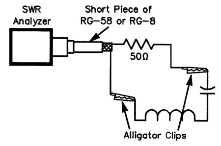
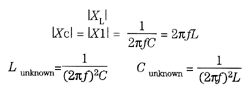
At resonance, the SWR known will be 1:1 with a 50-Q resistance, as reactance is zero. If either L or C isknown: (View)
View full Circuit Diagram | Comments | Reading(623)
BATTERY_MONITOR
Published:2009/6/22 18:01:00 Author:May

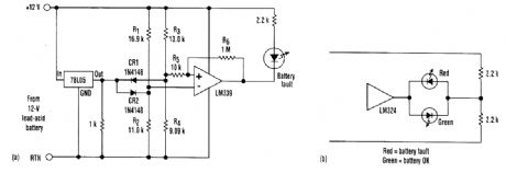
One typical application for the detector involves monitoring a lead-acid battery. It indicates a fault when the battery voltage is outside an 11- to 14-V window. Because the circuit is powered by the battery, the input and reference were switched to keep the comparator inputs within its common-mode range.The circuit's reference is 5.0 V. The resistor values in divider, R1/R2 were selected to produce 5.5 V at the inverting input when the battery voltage is 14.0V. Divider R3/R4 is set to produce 4.5 V at the noninverting input when the battery voltage is equal to 11.0V.When the battery voltage is within the window, the noninverting input is more positive than the inverting input which is clantped at 4.5V by CR2, the noninverting input continues below that, the comparator's output goes low, and the LED turns on. When the battery voltage rises above 14V, the noninverting input is clamped at 5.5V by CR1, the inverting input continues above that, the com-parator output again goes low, and the LED turns on. Resistors R5 and R6 show that hysteresis might be added to this circuit in a conventional manner.If an op amp, such as an LM324 is used as the comparator, two LEDs can be implemented. The green LED will tum on when the battery voltage is within the window, and the red LED tums on when the battery voltage is outside the window. (View)
View full Circuit Diagram | Comments | Reading(2)
Low cost Wien oscillator composed of F007
Published:2011/7/28 3:16:00 Author:Ecco | Keyword: Low cost , Wien oscillator

The chart shows the low cost Wien oscillator circuit. One hand, the circuit can avoid the problem of having to adopt expensive inductors in the general oscillator circuits. On the other hand,it can also avoid using double-potentionmeter to adjust frequency in the Wien bridge oscillators. It only uses a potentiometer to adjust the frequency, so the cost is lower. The adjusting frequency range is small, although there are some defects, it can still be used when it needs small frequency range, and the circuit is stable. (View)
View full Circuit Diagram | Comments | Reading(590)
Wien bridge sine-wave generator
Published:2011/7/28 2:19:00 Author:Ecco | Keyword: Wien bridge , sine-wave, generator

Oscillation frequency of the circuit shown in the figure is about lkHz, and it uses the regulator 2DW78 to stabilize amplitude. Ifl. 5kΩ resistors in the bridge isreplaced bycoaxial double potentiometer, the band switch needs to access different capacitors, the output signal frequency can be adjusted continuously. The maximum frequency of oscillation circuit is decided by the characteristics of operational amplifier F007. And the greater resistance, capacitance on low frequency end will cause instability or leakage, so the input impedance of operational amplifier should be as high as possible.
(View)
View full Circuit Diagram | Comments | Reading(792)
HIGH_CURRENT_DRIVE_CIRCUIT_FOR_SINGLE_HETEROSTRUCTURE_LASER_DIODES
Published:2009/6/22 18:01:00 Author:May


The transistor is operated in the avalanche mode. You might need to try several 2N2222 devices before finding one that oscillates. R2 is adjusted for optimum oscillation. This supply provides pulse of 10 to 20 amps at about 50 ns. (View)
View full Circuit Diagram | Comments | Reading(756)
Fan speed controller diagram 1
Published:2011/6/27 20:25:00 Author:Nora | Keyword: Fan , speed , controller

Step-down power supply circuit consists of the capacitor Cl, rectifier diodes VDl, VD2, filter capacitor C2, the power indicator light-emitting diode composed of VL and VS regulator diode.Controlled oscillator consists of a time-base integrated circuit IC, resistors RI, R2, capacitors C3, potentiometer RP and diode VD3, VD4 formed.Control implementation of the circuit consists of the fan motor M, thyristor VT, resistor R3 and the first 3 feet inside the IC circuit.AC 220V voltage buck by Cl, VDl and VD2 rectified, VL and VS filtered and C2 regulated, the IC provides about 8V DC voltage.Controlled oscillator work, a 3-pin output from the IC cycle 105, the duty cycle adjustable oscillating pulse signal, the use of this pulse signal to control the conduction status of thyristor VT.Adjust the resistance of RP, you can change the pulse duty cycle (adjustment range of 1% -99%), control the level of the fan motor M speed, resulting in simulated natural wind (gusts period of 10s).Change the capacitance of C3, can change the oscillator weeks moon, thus changing the simulation of natural wind cycle. (View)
View full Circuit Diagram | Comments | Reading(2462)
SOUND_SUBCARRIER_GENERATOR
Published:2009/6/22 17:59:00 Author:May


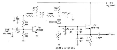
This circuit will generate an FM sound subcarrier at 4.5 or 10.7 MHz for FM and TV IF testing and alignment. Q1 is an audio amplifier and Q2 is a VCO rrtodulated by an MV2112 varactor. Devia-tion up to 1% of frequency can be obtained. L is chosen to resonate with the circuit capacitance to either 4.5 or 10.7 MHz. The values will be around 2 to 10 pH, depending on the frequency. (View)
View full Circuit Diagram | Comments | Reading(773)
| Pages:1393/2234 At 2013811382138313841385138613871388138913901391139213931394139513961397139813991400Under 20 |
Circuit Categories
power supply circuit
Amplifier Circuit
Basic Circuit
LED and Light Circuit
Sensor Circuit
Signal Processing
Electrical Equipment Circuit
Control Circuit
Remote Control Circuit
A/D-D/A Converter Circuit
Audio Circuit
Measuring and Test Circuit
Communication Circuit
Computer-Related Circuit
555 Circuit
Automotive Circuit
Repairing Circuit