
Circuit Diagram
Index 1391
LIGHT_SWITCHED_LED_BLINKER
Published:2009/6/22 22:42:00 Author:May

This circuit can be used to flash an LED during periods of darkness.Use it for burglar alarm simulators for boats,docks,autos,etc. (View)
View full Circuit Diagram | Comments | Reading(606)
HEARTBEAT_MONITOR
Published:2009/6/22 22:42:00 Author:May

An IR photodiode, which senses IR skin reflectivity as a result of increased blood volume during the periods that the heart forcibly contracts, is used to pick up a signal that is correlated with the heartbeat. A transistor and op amp raise this to a level suitable to trigger logic circuitry or to be displayed on a scope. (View)
View full Circuit Diagram | Comments | Reading(5287)
PHONE_PAGER
Published:2009/6/22 22:42:00 Author:May

This pager allows you to use your in-house phone wiring as a PA system. It uses two tone decoders to detect a particular touch-tone key. This key enables an audio amplifier. (View)
View full Circuit Diagram | Comments | Reading(2161)
PROGRAMMABLE_CAPCITOR_CIRCUIT
Published:2009/6/22 22:42:00 Author:May

IC1 CD4066 quad bilateral switchG1 10-μF, 25-V capacitorC2 22-μF, 25-V capacitorC3 47-μF, 25-V capacitor04 100-μF,25-V capacitorC5 1-μF, 25-V capacitor06 0.1-μF, 25-V capacitorThe programmable capacitor can be very useful in circuits where you need to switch capacitance values. Remember that the ON resistance of IC1 appears in series with the capacitors and must be taken into account in some applications as it is not negligible.
(View)
View full Circuit Diagram | Comments | Reading(591)
ADC_BUFFER
Published:2009/6/22 22:42:00 Author:May
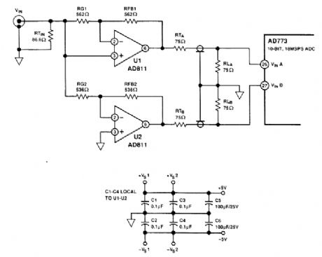
Useful for driving high-speed, 10-bit ADCs, this circuit was developed to drive an 18-MSPS 10-bit ADS. It works from ±5-V supplies. (View)
View full Circuit Diagram | Comments | Reading(637)
PHOTODIODE_ANIPLIFIEB
Published:2009/6/22 22:41:00 Author:May

A photodiode amplifier combined with a dc-restoration circuit will reject low-frequency ambient backgroud,easing measurement of a light signal. (View)
View full Circuit Diagram | Comments | Reading(1729)
WIDEBAND_GENERAL_PURPOSE_BUFFER
Published:2009/6/22 22:41:00 Author:May
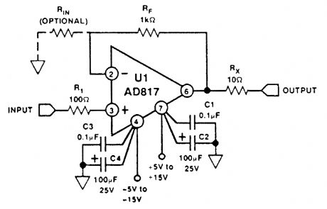
This circuit has unity gain and response up to 70 MHz. UI is an Analog Devices AD817. (View)
View full Circuit Diagram | Comments | Reading(644)
LOU_NOISE_LIGHT_SENSOR_WITH_dc_SERVO
Published:2009/6/22 22:40:00 Author:May
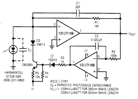
View full Circuit Diagram | Comments | Reading(1090)
SUPPRESS_JITTER_WITH_HYSTERESIS
Published:2009/6/22 22:40:00 Author:May

When the comparator's output changes its state from low to high, the rising edge of the output pulse, differentiated by the C1/R1 chain, opens Q1. This blocks comparator M via its strobing input and sustains its output in the H state for a period of time, defined by the time constant R,Ct After C1 is charged by the current flowing through R1, Q1 is shut off and the comparator is released. When the comparator's output state changes from high to low, a similar process, involving elements R2, C2, and Q2, occurs. In many applications, the output transition in only one direction is of vital importance, and the elements, which provide temporal hysteresis for the opposite direction transition, can be omitted. (View)
View full Circuit Diagram | Comments | Reading(609)
OPTICAL_FRINGE_COUNTER
Published:2009/6/22 22:39:00 Author:May
For work with interferometer and optical experiments, this fringe counter can be useful. Photo transistor Q1 provides light and dark sensing. As the sensor is moved across the fringe pattern alternate light and dark areas translate to an electrical waveform. This is amplified by IC1 and counted by IC2. A Schmitt trigger circuit can be added, if desired. (View)
View full Circuit Diagram | Comments | Reading(3027)
10_MHz_FREQUENCY_STANDARD
Published:2009/6/22 22:39:00 Author:May

A Radio Shack 10-MHz receiver is used as a basis for this circuit. The L.O. and IF frequencies are added. When the receiver is tuned to 10 MHz(WWV), the sum of the L.O. and IF are used to phase lock a VCO to the 10-MHz signal. By using a divider in the Ioop, 2.5 or 5 MHz can be used as well. (View)
View full Circuit Diagram | Comments | Reading(921)
HI_Z_MICROPHONE_BUFFER_AMPLIFIER
Published:2009/6/22 22:39:00 Author:May
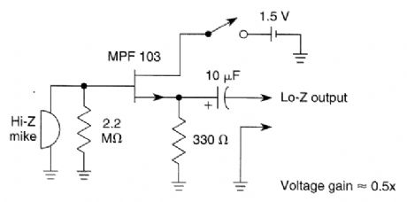
A low impedance output from a high-Z microphone can be obtained with this circuit. No voltage gain is obtained, but a power gain is obtained because the output impedance is much lower (300 Ω), with -6-dB voltage gain. (View)
View full Circuit Diagram | Comments | Reading(776)
UNITY_GAIN_ADC_BUFFER
Published:2009/6/22 22:39:00 Author:May
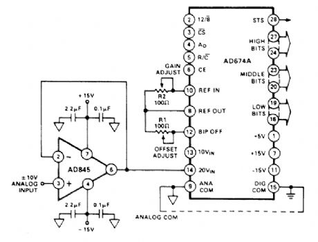
This buffer is suitable for ADCs of 12 bits bandwidth of 5μs or greater.The wide bandwidth of the AD845 ensures a low output impedance at higher frequencies in the voltage follower (buffer) configuration. (View)
View full Circuit Diagram | Comments | Reading(593)
SUN_TRACKING_CIRCUIT_FOR_SOLAR_ARRAYS
Published:2009/6/22 22:38:00 Author:May


The sun tracker uses a combination of three photoresistors. R7, R8, and R9, to ensure that the circuit will follow the sun during the day, but not look for it at night. Photoresistor cells, R7, R8, and R9 have a value of 160Ω in full sunlight and 4880 Ω in the shade, that is not absolutely critical. R7 is mounted in a well with a narrow slit so that sunlight falls upon it only when the photoresistor is pointed directly at the sun. When that occurs, the resistance of R7 drops. That photoresistor and potentiometer R4 form a voltage divider at the base of the Darlington transistor, Q1. When R7's resistance is low, Q1 will be kept off.
When the sun swings a little westward, R7 will no longer be in sunlight, causing its resistance to go up, which raises the base voltage of Q1 and turns that Darlington on. That, in turn closes the relay, K1, providing current to the drive motor, MOT1, which is a 1.5-Vdc, low-torque hobby motor. The motor then turns slowly (resistor R6 limits the maximum current to the motor and keeps it from running too fast), putting R7 in dire'ct sunlight again; Q1's base voltage then drops and the tracker stops. That is repeated again and again as the sun moves across the sky. Photoresistor R8 is mounted on the outside of the well so that it receives a wide angle of full sunlight. When the sun is shining, R8's resistance is low, keeping Q2 turned off, and allowing the tracker to act as described, without interference. But if the sun slips behind a cloud, R8's resistance goes high, producing a forward bias on the base of Q2.That turns that transistor on and sinks the base of Q1 to near ground so that Q1 then remains off. That immobilizes the tracker drive; that also keeps the drive shut down in the dark of night.
Photoresistor, R9, is the dawn sensor. It is mounted on the back of the sun tracker. When the tracker stops at sunset, pointing toward the west, R9 is pointing toward the east. When the sun rises the following morning and shines on R9, its resistance goes low, turning Q2 off and allowing Q1's base to go high. That presents current to the relay and therefore to the drive motor, causing the tracker to swing around to the east. (View)
View full Circuit Diagram | Comments | Reading(4814)
TELEPHONE_SCRAMBLER
Published:2009/6/22 22:38:00 Author:May

Two hybrids (T1 and T2) are used to allow direct connection to a telephone line. This circuit uses the common speech-in-version algorithm where the frequency of an audio signal is inverted about a center frequency. An LM1496 balanced modulator is used to heterodyne the specch range against a 3.58-kHz signal. (View)
View full Circuit Diagram | Comments | Reading(6)
TACHOMETER_ADAPTER
Published:2009/6/22 22:36:00 Author:May
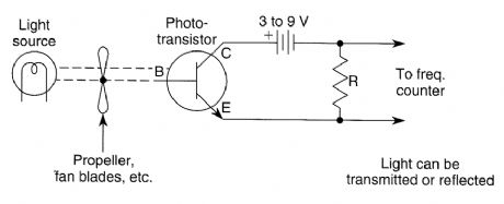

Use of a phototransistor and light source can enable a frequency counter to act as a tachometer:The light source is interrupted by the number of propeller blades, fan blades, spokes, or other marking. R can be anywhere from 1 to 100 kΩ. Try several values for best results. (View)
View full Circuit Diagram | Comments | Reading(1058)
TELEPHONE_VOICE_MAIL_ALERT
Published:2009/6/22 22:36:00 Author:May

The circuit is built around a couple of low-cost ICs: an H11C4 optoisolator/coupler with an SCR output (U1) and an LM3909 LED flasher (U2). It is connected to the phone line in the same manner as any extension phone. A ring signal on the telephone activates the optoisolator/SCR, and causes U2 to flash LED1. This flash signifies that a ring signal has been received. (View)
View full Circuit Diagram | Comments | Reading(1561)
TRAFFIC_LIGHT_SEQUENCER_CIRCUIT
Published:2009/6/22 22:36:00 Author:May
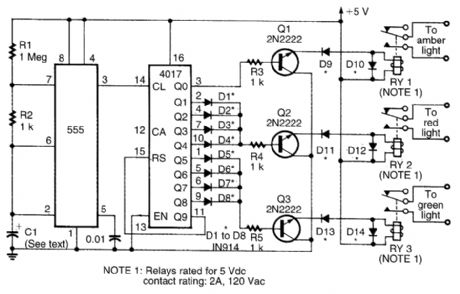
This circuit uses a 555 timer to drive a 4017 counter. The counter outputs drive transistor relay drivers. Time lights on can be proportioned by changing connections of outputs of counter. (View)
View full Circuit Diagram | Comments | Reading(4869)
ACOUSTIC_FIELD_GENERATOR
Published:2009/6/22 22:35:00 Author:May
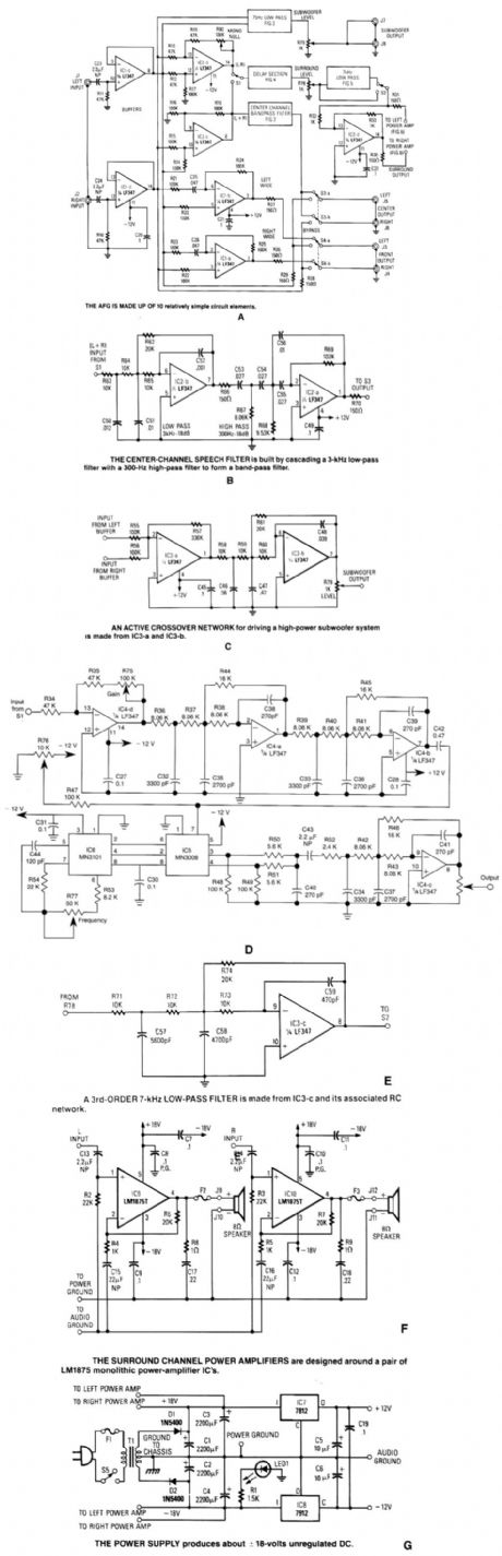
Referring to the simplified schematic in A, the AFG is made up of 10 relatively simple circuit el-ements. ICl-c and ICl-d are configured as unity-gain noninverting buffer amplifiers.
The summing (L+R) amplifier, IC2-c, combines equal amounts of the left and right signals, via R14 and R15, to develop a total composite signal. Left- and right-channel signals are applied equally through R13 and R12 to IC2-d, the difference (L-R) decoder. Any common to both channels is canceled by IC2-d, which exactly balances the inverting and noninverting gains of the amplifier for a perfect null.
The stereo width-enhancement circuit made up from IC1-a and IC-b works similarly to the (L-R) decoder, except that C25 and C26 have been added in the inverting inputs of each op amp. IC1-b de-velops the left wide signal because its inverting and noninverting inputs are connected to the left
and right channels opposite that of IC1-a. The output of the width-enhancement circuit is routed to 54, which selects either the wide or the bypass signal for feeding the front-channel amplifier.
The center-channel dialogue filter is built by cascading a 3-kHz low-pass filter with a 3-Hz high-pass filter to form a band-j:ass filter. It has a sharp -18 dB/octave cutoff, a flat voltage and power fre-quency response, and minimum phase change within the passband.
In C, IC3-a and IC3-b form an active crossover network for driving a subwoofer. IC3-a sums sig-nals from the left- and right-channel buffer amps, it inverts the summed signal 180 degrees, and pro-vides a low driving impedance for the following filter stage. IC3-b and its associated RC network form a 75-Hz, 3rd-order low-pass filter. The filter inverts the signal another 180 degrees, so the signal that appears across R79 (which is the output-level control) is back in phase with the original input signal.
The delay section of the AFG, shown in D, is built around the MN3008 bucket brigade device (BBD), and the MN3101 two-phase variable-frequency clock generator. The amount of delay re-quired in this system varies between approximately 5 to 35 milliseconds. The delay time of a BBD is equal to the number of stages divided by twice the clock frequency. Values were chosen for R53, R54, R77, and C44, to produce a clock frequency, adjustable via R77, which varies from about 30 kHz to 130 kHz.
In A, S1 selects the signal to be delayed, either the difference signal (L-R) from IC2-djn the ma-Lrix mode or the sum signa! (L-R) from IC2-c in the concert mode. The selected signal is fed from S1 to the delay section (D) where IC4-d is configured as an inverting amplifier; R75 adjusts the gain between unity and X3: Integrated circuits IC4-a and IC4-b, along with their assoicated RC networks: are identical 3rd-order 15-kHz low-pass filters. Cascading two filters produces a very sharp cut off (-36 dB per octave). Potentiometer R76 adjusts the bias voltage required by the BBD to exactly one half the supply voltage, as required.
The power suppty of the AFG, shown in G, is of conventional design. A 25-V center-tapped trans-former, along with diodes D1 and D2, produces about t18-V unregulated dc. 1bro 2200-μF filter capacitors provide ample energy storage to meet the high-current demands of the audio output amplifier ICs during high output peaks. (View)
View full Circuit Diagram | Comments | Reading(1290)
BRIDGE_AMPLIFIER_WITH_LOW_NOISE_COMPENSATION
Published:2009/6/22 22:35:00 Author:May
View full Circuit Diagram | Comments | Reading(829)
| Pages:1391/2234 At 2013811382138313841385138613871388138913901391139213931394139513961397139813991400Under 20 |
Circuit Categories
power supply circuit
Amplifier Circuit
Basic Circuit
LED and Light Circuit
Sensor Circuit
Signal Processing
Electrical Equipment Circuit
Control Circuit
Remote Control Circuit
A/D-D/A Converter Circuit
Audio Circuit
Measuring and Test Circuit
Communication Circuit
Computer-Related Circuit
555 Circuit
Automotive Circuit
Repairing Circuit