
Circuit Diagram
Index 1394
2.5kHz Wien bridge signal generator
Published:2011/7/28 2:16:00 Author:Ecco | Keyword: 2.5kHz , Wien bridge , signal generator
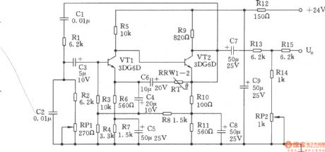
The 2.5kHz signal generator is a RC Wien low-bridge oscillator circuit, it is shown as the chart. Transistor VTl, VT2 form second order direct coupled amplifier.By inputting the bootstrap can improve the circuit's input impedance and decrease the impact on RC shift circuit. Connecting a T-attenuation device on output end can meet the requirement of inpedance output on one hand, on the other hand it also can reduce the influence of load on Rc shift circuit. Taking the measures, the oscillator frequency stability is mainly decided by the RC phase shift components. Rc components with low temperature coefficient is used, thus, the oscillator frequency is relatively stable (25 ℃ ± 15 ℃, the frequency changing ≤ ± 5Hz).
(View)
View full Circuit Diagram | Comments | Reading(1465)
SIMPLE_HARMONIC_DISTORTION_ANALYZER
Published:2009/6/22 17:54:00 Author:May


This simple circuit lets you accurately measure the total harmonic distortion(THD)using your true-RMS voltmeter.This THD circuit is somewhat different from the usual types: it can operate at the standard fre-quency of 1000 Hz, but it also is tunable from 970 Hz to 1030 Hz, and has an adjustable Q factor of 0.3 to over 50. Op-amp UI, a TLC272 CMOS unit, contains the two voltage-followers required to buffer the input to the bootstrapped twin-T notch filter. Tuning is accomplished by R1, R2, and R3, which are standard linear-taper slide pots ganged together by mounting them side-by-side and glu-ing their sliders together.The only other intportant construction hint is to use twisted pair at the cir-cuit's input and output.To calibrate the circuit, input a 1000-V RMS signal at 2000 Hz, set 51 to TEST, and adjust R7 for a reading of 0.99-V RMS on a true-RMS voltmeter at the output.To use the circuit, set 51 to TUNE, input a 1000-Hz sine-wave signal to the amplifier under test, and set the amplifier's output to the THD adapter and tune R1/R2/R3 for the lowest output signal.Then, set 51 to TEST and read the RMS voltage. To calculate the percent THD use: (View)
View full Circuit Diagram | Comments | Reading(1566)
Color TV pincushion correction circuit diagram 1
Published:2011/7/21 1:42:00 Author:Ecco | Keyword: Color TV , pincushion correction

Field excitation pulses is applied directly to the pin 13 of N402 (TA8859) to trigger monostable trigger, then it generates a constant field frequency pulse-width pulse, which can control field sawtooth wave generating circuit after shaping, the N402 (15) pin is connected externally C418 capacitor with constant current charging to form a sawtooth wave current. Sawtooth amplitude and charging speed is controlled by the AGC circuit of N402, which can meet the needs of 50Hz/60Hz. Sawtooth wave produced by the field sawtooth wave circuit is made a series of linear correction by the N402, then pin (8) will output field excitation pulse.
(View)
View full Circuit Diagram | Comments | Reading(1041)
SIMPLE_SIGNAL_GENERATOR_FOR_SIGNAL_TRACING
Published:2009/6/22 17:50:00 Author:May

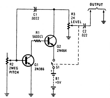
A simple R-C oscillator generates a harmonic-rich waveform for signal injection. (View)
View full Circuit Diagram | Comments | Reading(772)
Tube Power Amplifier circuit diagram(with power source)
Published:2011/7/20 20:09:00 Author:Ecco | Keyword: Tube Power Amplifier , power source
If the power amplifier coupled with good speakers and good environment, and DVD audio playback, it likes the power amplifier with the price in a few thousand dollars. The following is the power circuit diagram:
(View)
View full Circuit Diagram | Comments | Reading(676)
ANALOG_CIRCUITRY_CALIBRATOR
Published:2009/6/22 17:47:00 Author:May


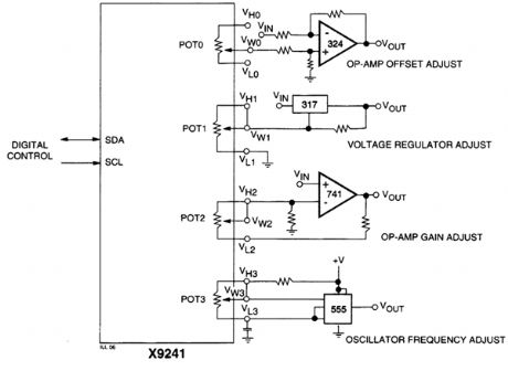
An XICOR X9241 Quad POT IC can be used to digitally adjust four analog circuits, as shown in the example schematic. (View)
View full Circuit Diagram | Comments | Reading(810)
Sensor detector circuit diagram
Published:2011/7/20 20:08:00 Author:Ecco | Keyword: Sensor detector
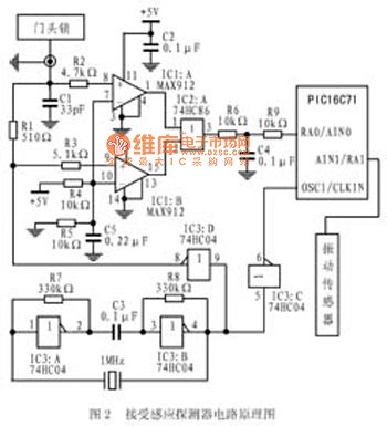
Figure 1 shows the the proximity sensor detector circuit temperature compensation which is composed of MAX912. In the circuit, the door lock (or 200cm2 Bonded Copper) is used as a capacitor plate composed of a sensing surface. When the body is approached the other plate, the capacitance value will increase with the closing of the body (range between 2pF to 5pF). When the body is 20cm far away from the door lock, it can generate approximately 2pF capacitance. The 74HC04 and crystal oscillator will generate 1MHz square wave signal, which is all the way sent to the microcontroller PIC16C71 as the oscillation signal; another way is sent to the proximity sensor detector circuit.
(View)
View full Circuit Diagram | Comments | Reading(1331)
ANALOG_DE_GLITCH_CIRCUIT
Published:2009/6/19 5:13:00 Author:May


Low-frequency signals produced by transducers, measurement equipment, or data loggers often appear like the first waveform in the figure. The circuit shown operates as a tracking sample-hold, and the transients are replaced in the output by the stored value of the current signal at the instant of the transient.
The input signal is buffered and inverted by ICla, and the differentiated result shown at 2 ap-plied to the inputs of two comparators IC2-a and IC?-b. VR1 and VR2 set levels to prevent false or unnecessary operation. Either comparator output triggers the mono IC3 from positive or negative signal transients. When IC3 has not been triggered, TRI and TR2 'p' channel JFETs are on, and IClb operateb as an integrator with a high leakage, and tracks the input signal. When the mono is trig-gered as at 3, TRI and TR2 turn off and the previous signal value is held constant, as shown at 4. The resulting output waveform can then be easily filtered to remove the harmonics from the restoring step at the end of the mono period, if needed.
The criteria for successful operation are:
t2 > t1 (mono period longer than glitch)t2/T small (to optimize output waveform) Signal bandwidth Signal phase
The signal range is approximately ±5V, depending on the tfansient amplitude and polarity. The mono period shown is 100 mS, but this can be optimized in practical applications. The shorter the mono period in relation to the signal waveform, the better the quality of the result. (View)
View full Circuit Diagram | Comments | Reading(1234)
Optical communication receive circuit diagram
Published:2011/7/21 3:06:00 Author:Ecco | Keyword: Optical communication receive

When the phototube is exposured by the light that emits from light-emitting diode modulated by proper infrared transmitter(the transmitter is far away from 137.2 m). The circuit can give the maximum output of 500 mW to 15 Ω speakers. The system is applicable to installing electronic wire wireways in inconvenient situation and useing under the sistuation of wavelength in about 0.9 μ m. (View)
View full Circuit Diagram | Comments | Reading(1632)
VIDEO_PREAMP
Published:2009/6/19 5:04:00 Author:May

An NE592 or LM733 is used as a general-purpose video amplifier in this schematic. J2 and J3 provide two anti-phase outputs. R2 is a gain control. The bandwidth is about 100 MHz. (View)
View full Circuit Diagram | Comments | Reading(4)
900w full-wave circuit diagram
Published:2011/7/21 3:07:00 Author:Ecco | Keyword: 900w full-wave

This circuitry is composed ofbidirectional triode thyristor controlled silicon delivered by unijunction transistor striking on rocks and bridge rectifier. It can provide wide range of control to resistive load by RT. The pulse transformer T makes bidirectional Hiccup controlled silicon polar and unijunction transistor steady - state current be separated.
(View)
View full Circuit Diagram | Comments | Reading(784)
VIDEO_SELECTOR
Published:2009/6/19 5:00:00 Author:May

This circuit selects one of two channels with a logic signal. The unused channel is shorted out, which minimizes crosstalk. The bandwidth at -3 dB is about 8 MHz. It is advisable to buffer this cir-cuit because there is some loss in the switches when feeding a 75-Ω load. (View)
View full Circuit Diagram | Comments | Reading(4)
ION_DETECTOR
Published:2009/6/19 4:59:00 Author:May
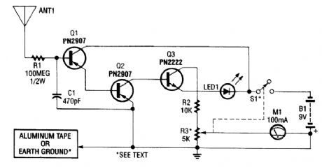
This circuit detects static charges and free ions in the air. It can be used to indicate the presence of ion emissions, high-voltage leakage, static electricity, electrostatic fields, etc. The ground connection is made by either an earth ground or by touching the aluminum foil electrode with your hand.M1 is a 100-μA meter. R3 is a sensitivity control. (View)
View full Circuit Diagram | Comments | Reading(3454)
COMBINATION_SYNC_STRIPPER_AND_UNIVERSAL_VIDEO_INTERFACE
Published:2009/6/19 4:59:00 Author:May

This combination sync stripper and universal video interface can solve a lot of problems for you, including Super-Nintendo-to-anything interfacing, video overlay and scope TV frame locking. Kits, fully tested units, and custom cable assemblies are available through Redmond Cable. This unit uses an LM1881 (NS) synch separator IC. (View)
View full Circuit Diagram | Comments | Reading(4273)
AUDIO_LIMITER
Published:2009/6/19 4:59:00 Author:May

An optoisolator is used as an attenuator in this circuit. When the LM386 draws more current on audio signals, the 2N3638 turns on, which biases the optoisolator on, and reduces the volume. (View)
View full Circuit Diagram | Comments | Reading(1988)
2NEGATIVE_ION_GENERATOR
Published:2009/6/19 4:58:00 Author:May
In this circuit, air is circulated past a pointed electrode that has a high negative voltage applied to it. The transformer is a small 4- to 6-kV output type with a filament winding. A good source of parts is a discarded electronic bug catcher. (View)
View full Circuit Diagram | Comments | Reading(954)
VIDEO_dc_RESTORE_CIRCUIT_
Published:2009/6/19 4:58:00 Author:May

This circuit restores the black level of a monochrome composite video signal to 0 V at the beginning of every horizontal line. This circuit is also useful with CCD scanners to set the black level. (View)
View full Circuit Diagram | Comments | Reading(1262)
ION_SENSING_ELECTROSCOPE
Published:2009/6/19 4:57:00 Author:May
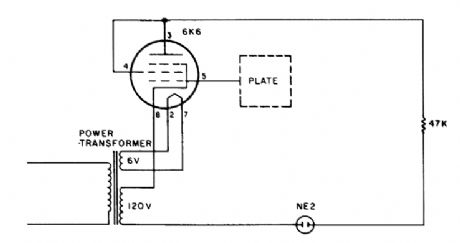
Negative ions are sensed by a plate antenna. A negative charge induced on the plate cuts off a vacuum tube, causing the neon indicator to go out. (View)
View full Circuit Diagram | Comments | Reading(999)
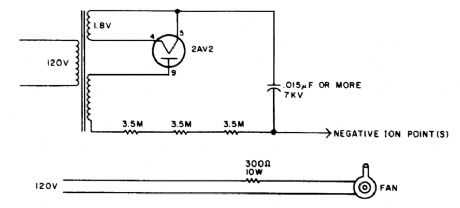
1NEGATIVE_ION_GENERATOR
Published:2009/6/19 4:56:00 Author:May

An NE555 drives a Darlington connected pair of transistors. T1 is a small high-voltage trans-former or auto ignition coil, B/W TV flyback, etc. C3, C4, and D1 must be rated for 10 to 15 kV. The fan blows air across the discharge point. (View)
View full Circuit Diagram | Comments | Reading(2617)
RADIO_COMMERCIAL_ZAPPER
Published:2009/6/19 4:55:00 Author:May

The L&R inputs are summed, dated and drive a comparator. The comparator senses level and generates a transition when audio inputs go above or below preset thresholds. The number of these transitions (corresponding to rapid volume changes) are integrated and feed voltage controlled amplifiers. This device actually senses dynamic range. (View)
View full Circuit Diagram | Comments | Reading(927)
| Pages:1394/2234 At 2013811382138313841385138613871388138913901391139213931394139513961397139813991400Under 20 |
Circuit Categories
power supply circuit
Amplifier Circuit
Basic Circuit
LED and Light Circuit
Sensor Circuit
Signal Processing
Electrical Equipment Circuit
Control Circuit
Remote Control Circuit
A/D-D/A Converter Circuit
Audio Circuit
Measuring and Test Circuit
Communication Circuit
Computer-Related Circuit
555 Circuit
Automotive Circuit
Repairing Circuit