
Circuit Diagram
Index 1399
Precision electric bridge isolation amplifier circuit composed of ISO100
Published:2011/6/26 22:16:00 Author:Rebekka | Keyword: Precision electric bridge , isolation amplifier

The precision electric bridge isolation amplifier circuit composed of ISO100 is mainly used for weighing, pressure measurement systems. ISO100 is a small, inexpensive optical isolation amplifier, the internal LED light passes the excitation and the optical receiver tube receives transmission. Figure shows the the main applications of the precision electric bridge isolation amplifier circuit. The bridge outputs 0 ~-l0mV unipolar signal. It is firstly amplified for 100 times by INA101 precision instrumentation amplifier, and then sent through the 100kΩ resistor Rl unipolar input ISO100 to ensure linear operation of the ISO100. (View)
View full Circuit Diagram | Comments | Reading(932)
CFl55 Series dual power high input impedance single op amp circuit diagram
Published:2011/5/15 6:16:00 Author:Rebekka | Keyword: dual power , high input impedance , single op amp

The input circuit of CFl55 series op-amp is composed of the FET. The features are: It has a very small input current, low supply current, low power consumption, low noise, its offset voltage is small, peripheral-zero side. The series can be used for high-speed integrators, the sample and keeping circuit of fast D / A converter etc. Its similar or direct substitution models are: CFl55MT, CF255LT, CF355CT, CFl55MD, CF255LD, CF355CD, CFl55MJ, CF255LJ, CF355CJ, CF355CP and so on. The CFl55 typical application circuit is shown as above. Figure (a) is the inverting amplifier and the zeroing circuit. Figure (b) is the differential input and zeroing circuit. (View)
View full Circuit Diagram | Comments | Reading(443)
100_W_VARIABLE_RESISTOR_SIMULATOR
Published:2009/6/19 4:09:00 Author:May

Variable resistive loads with precise load steps often are required in automatic testers used to test and calibrate power supplies. The action of a high-power(100 W)variable resistor can be simu-lated with the circuit shown.The voltage drop across R1, which is proportional to the FET current, is compared against a vari-able input voltage reference using a high-gain op amp. Error voltage developed by the amplifier drives the gate, controlling the transconductance of the FET.Power dissipation is limited by the safe-operating-area curve of the selected FET. The FET should be mounted onto a properly sized heatsink or a heatsink-fan combination to maintain its case temperature within safe limits. The circuit is designed to dissipate a ntaximum power of 100Wif the FET-case temperature is maintained below 50℃. The potentiometer (RV1) can be replaced by a dig-ital-to-analog converter so that it can adapt to the computer control for use in automatic testers. (View)
View full Circuit Diagram | Comments | Reading(1311)
LOW_POWER_20_METER_CW_TRANSMITTER
Published:2009/6/19 4:09:00 Author:May
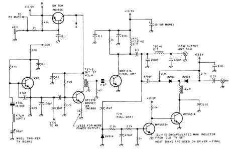
The transmitter has a VXO circuit to drive an amplifier that is keyed. The keyed amplifier drives an MRF 476 final amplifier, which delivers about 2-W output. A solid-state T-R switch is included for the receiver. The parts values shown are for the 20-me-ter band. (View)
View full Circuit Diagram | Comments | Reading(1381)
Op amp common-mode voltage breakdown input stage and its protection measure circuit diagram
Published:2011/5/17 2:45:00 Author:Rebekka | Keyword: Op amp , common-mode voltage, breakdown input stage, protection measure

There is a current of the transistor collector junction flow from basal pole to collecting anode. If the source of resistance passes from feet 2 or feet ③ is low, then the collector junction current will be very large, and the input stage transistors will be damaged. In this case, remove the power supply voltage, and the signal source is not removed. The common-mode input will damage the ntegrated operational amplifier. Another case that makes the integrated operational amplifier common mode input failure is that the signal source has capacitive elements. The capacitance is charged to the high level of the signal source, remove the supply voltage and signal at the same time. Because the existance of charging voltage of the signal source capacitance, it is equivalent to the existance of signal source voltage. If the capacitor is greater than 0.1μF. The discharge current of the capacitor can burn the transistor. (View)
View full Circuit Diagram | Comments | Reading(1031)
SINGLE_TONE_INFRARED_CONTROL_TRANSMITTER
Published:2009/6/19 4:07:00 Author:May

A modulated beam of IR light is produced by this transmitter. This circuit can be used for on/off controls or tone (CW) communications. The pot can be replaced by several pushbuttons and resis-tors, as shown for multitone applications. (View)
View full Circuit Diagram | Comments | Reading(569)
TV_REMOTE_CONTROL_RELAY
Published:2009/6/19 4:06:00 Author:May

This circuit functions as an IR repeater to extend the range of your TV remote control. MOD1 is a P/N GP1U52X IR detector and the receiver is available as Radio Shack P/N 276-137. (View)
View full Circuit Diagram | Comments | Reading(2516)
Digital frequency shift demodulator(CA3020、MC723、MC724)
Published:2011/7/18 20:22:00 Author:zj | Keyword: Digital, frequency shift, demodulator
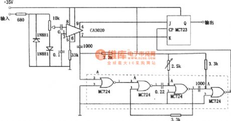
As shown in the figure it is the digital frequency demodulation circuit. The circuit can be used in 1kHz to 10kHz frequency range, and can be demodulated to the 1% frequency offset. The input stage of the circuit is composed of wide band amplifier CA3020. The differential output is added to the J-K input end of J-K trigger. Gate circuit MC724 constitutes the monostable multivibrator. Monostable multivibrator timing cycle is equal to the center frequency of the half cycle. Input signal strobes trigger after being delayed by the monostable multivibrator. (View)
View full Circuit Diagram | Comments | Reading(554)
WIRELESS_IR_HEADPHONE_TRANSMITTER
Published:2009/6/19 4:04:00 Author:May
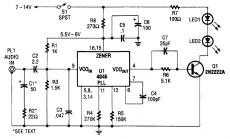
Audio input from PL1 frequency modulates the VCO section of a 4046 PLL chip. The VCO out-put drives Q1, a switching transistor. Q1 drives two IR LEDs. The signal produced is around 100 kHz, FM carrier VCO sensitivity is around 7.5 kHz/V. (View)
View full Circuit Diagram | Comments | Reading(4304)
ac_POWER_MONITOR
Published:2009/6/19 4:03:00 Author:May
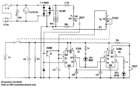
The 0-to 130-V voltmeter and neon AC PWR lamp provide an average indication of the ac power. The fuse and metal oxide varistor(MOV)protect the monitor against overvoltage spikes.Four 1N4004 diodes rectify the ac voltage, generating negative-going pulses twice per cycle(every 8.33 ms for 60-Hz power). Variable-resistor F1 supplies a reduced amplitude sample of these pulses to a missing pulse detector consisting of Q1, IC1, and associated circuitry. As long as the pulse amplitude exceeds the threshold value set by RI, IC1 continually triggers, keeping its output high.When the pulse amplitude drGps below the threshold value, IC1 times out with a time constant set by variable resistor R2 and the 0.47-μF capacitor. R2 is calibrated to read the number of cycles required for a dropout indication. It can be set between 1 cycle(about 17 ms)and 30 cycles(0.5 second).When IC1 times out, its output goes low. This turns on LED1. The low output also triggers IC2, which is configured as a set-reset flip-flop. This turns on LED2. When the voltage returns to normal, IC1 again starts triggering and its output returns high, turning off LED1. LED2, however, remains on until the manual reset button is pressed.The circuit is powered by a 9-V battery and is assembled in a plastic or grounded metal case. No-tice that thqre's no isolation between the ac power line and the monitor circuitry. Be careful to avoid electrical shock when testing the circuitry. (View)
View full Circuit Diagram | Comments | Reading(1629)
Call finder circuit
Published:2011/7/18 20:56:00 Author:zj | Keyword: Call finder

The work principle of the circuit: in the circuit, J1 is connected to the telephone line. When there is no call in, Vcc is 0V for there is no ringing signal. The circuit does not work with no power source voltage. When there is call in, the ringing signal is current limited by the R1, through C1, C6 coupling, bridge VD1 rectifier, C4 filter to supply power voltage Vcc for the whole device. By detecting, Vcc changes from 1.8V to 4.2V with ringing signal, but it does not affect the function. (View)
View full Circuit Diagram | Comments | Reading(883)
AUDIBLE_IR_DETECTOR
Published:2009/6/19 4:03:00 Author:May
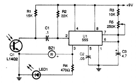
An IR-detector circuit offers an audible (as well as a visual) output, and also stretches the on time of the detected pulse to make the output easier to see, as shown.Photoresistor Q1 detects a remote's IR output pulse and sends a negative-going pulse to the trig-ger input (pin) of the 555IC, U1. The 555 is connected in a one-shot timer circuit; the output (pin 3) on time is set by the values of C3, R3, and R5 When an input pulse is detected, pin 3 goes high, lighting LED1 and activating the piezo buzzer, BZ1.For longer output pulses, set R5 to its maximum resistance value. To lengthen the circuit's on-time range, increase the value of C3, and to shorten the on-time range lower the value of C3. (View)
View full Circuit Diagram | Comments | Reading(981)
AUDIO_MODULATED_IR_TRANSMITTER
Published:2009/6/19 4:00:00 Author:May

This circuit produces an effect similar to frequency modulation (FM) by varying the voltage at pin 6 of the PLL using an audio signal. The FM 1R signal can be picked up by a receiver with an FM detector suitably tuned. (View)
View full Circuit Diagram | Comments | Reading(1115)
FM_RADIO_TRANSMITTER
Published:2009/6/19 4:00:00 Author:May

An FM radio generates an interference signal that can be picked up on another FM radio tuned 10.7 MHz above the first one. The 50-kΩ potentiometer adjusts the modulation level to maximum without distortion. The RC network improves the fidelity of the transmitted signal and provides dc isolation. The component values shown are provided as a starting point. They can vary somewhat for clifferent radios. Note that if you can't get the signal at 10.7 MHz above the frequency setting of the first radio, try tuning at 10.7 MHz below. Also, note that both tuned frequencies must be unused.Otherwise, you will hear your audio on top of the audio that is already there. You might have to play with both frequencies until you find two blank spots that are l0.7 MHz apart. (View)
View full Circuit Diagram | Comments | Reading(775)
LOW_POWER_40_METER_CW_TRANSMITTER_
Published:2009/6/19 3:59:00 Author:May

This CW transmitter has an output of up to 3 W. By using 24 V on Q2, up to 10 W output can be obtained. If a 24-V supply is used, Q1 must not see more than 12 V. Connect 12Vbetween junctions C3, R2 and L2, and remove L5. L1 should be a low-Q 18- to 20-μH inductor. R6 can be used (up to 47 Ω) to reduce the Q further. (View)
View full Circuit Diagram | Comments | Reading(2248)
LED_OUTPUT_INDICATOR_FOR_555_CIRCUITS
Published:2009/6/19 3:58:00 Author:May

A pair of LEDs connected as shown here can be used with just about any low-frequency 555 os-cillator to give high-/low-output indications. When the output goes high LED2 turns on, and when the output goes low LED1 tums on. (View)
View full Circuit Diagram | Comments | Reading(727)
RECEIVER_SIGNAL_STRENGTH_INDICATOR
Published:2009/6/19 3:58:00 Author:May

Using an AD606 log amplifier, this indicator gives a logarithmic output of +0.3 V at -80-dBm in-put to +3.5 V at 10-dBm input. Frequency range is to 50 MHz for this IC device. (View)
View full Circuit Diagram | Comments | Reading(977)
CURRENT_INDICATOR
Published:2009/6/19 3:57:00 Author:May

An LED requires 1.5 to 3 V across its terminals to light. This circuit uses a resistor shunt in series with source and load to produce this drop and cause the LED to Iight. At higher currents (>100 mA) use limiting resistors in series with LEDs to limit current to a safe value. (View)
View full Circuit Diagram | Comments | Reading(714)
MODEL_OAR_DERBY_WINNER_INDICATOR
Published:2009/6/19 3:56:00 Author:May

This derby-winner inc!icator uses infrared emitters and sensors to detect a car crossing the fintsh line. The first car to finish locks out the data from the second car, and the system can be reset by pressing S1. (View)
View full Circuit Diagram | Comments | Reading(710)
PERSONAL_MESSAGE_RECORDER
Published:2009/6/19 3:55:00 Author:May
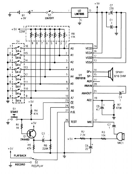
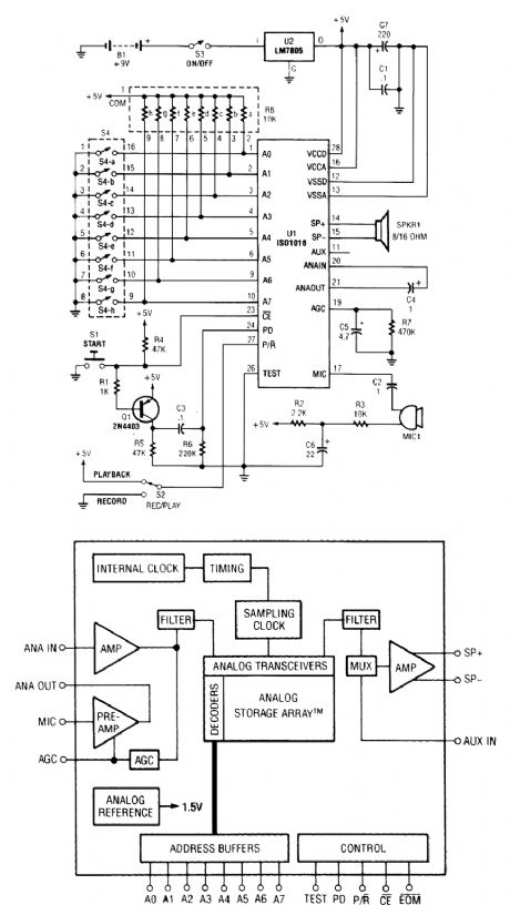
The personal message recorder is built around an ISD1016 CMOS voice messaging system, which does away with the cumbersome and expensive analog-to-digital and digital-to-analog con-version circuits.
A functional block diagram of the ISD1016 is shown. The ISD1016 contains all of the functions necessary for a complete message-storage system. The preamplifier stage accepts audio signals di-rectly from an external microphone and routes the signals to the ANA OUT (analog out) terminal. An automatic-gain control (AGC) dynamically adjusts the preamplifier gain to extend the input signal range. Together, the preamp and ACrC circuits provide a maximum gain of 24 dB. The internal clock samples the signal and, under the control of the address-decoding logic, writes the sampling to the analog-storage array. Eight external input lines allow the ISD1016's message space to be addressed in 160 equal segments, each with a 100-millisecond duration. When all address lines are held low, the storage array can hold a single, continuous, 16-second message.
However, there is a special addition to the POWER DOWN input (pin 24) of UI. If the internal mem-ory becomes full during recording, an overflow condition is generated in order to trigger the next de-vice. Once an overflow occurs, pin 24 must be taken high and then low again before a new playback of record operation can be started.
Transistor Q1, C3, R5, and R6 form a one-shot pulse generator that automatically clears any overflow condition each time that start switch (51) is pressed. Switch 52 selects either the playback or the record mode. Switch 54-an 8-position (a-h) DIP switch-is included in the circuit to allow the circuit's record/playback time to be varied from 0 to 16 seconds. The maximum time available is when al18 switch positions are closed (or set to the on position). Resistor network R8 (a-h) is in-cluded in the circuit to provide a pull-up function for the address lines, which thereby controls UI's record/playback time. (View)
View full Circuit Diagram | Comments | Reading(2032)
| Pages:1399/2234 At 2013811382138313841385138613871388138913901391139213931394139513961397139813991400Under 20 |
Circuit Categories
power supply circuit
Amplifier Circuit
Basic Circuit
LED and Light Circuit
Sensor Circuit
Signal Processing
Electrical Equipment Circuit
Control Circuit
Remote Control Circuit
A/D-D/A Converter Circuit
Audio Circuit
Measuring and Test Circuit
Communication Circuit
Computer-Related Circuit
555 Circuit
Automotive Circuit
Repairing Circuit