
Circuit Diagram
Index 1387
RECHARGEABLE_SOLAR_POWER_FOR_SUN_TRACKER
Published:2009/6/22 23:01:00 Author:May

This application circuit provides rechargeable solar power for the sun tracker, as well as for another 12-volt device. PC1 and PC2 can be mounted on sun tracker assembly. (View)
View full Circuit Diagram | Comments | Reading(1459)
ATMOSPHERE_NOISE_MONITOR
Published:2009/6/22 23:21:00 Author:Jessie

Tune an unmodified transistor radio to an unused frequency near 540 kHz that's free of broad-cast-station interference; the receiver is used to pick up sferics. The received signal is fed from the receiver's earphone jack through a patch cord to the input jack(J1)of the circuit. The back-to-back audio transformers, T1 and T2, provide a suitable impedance match and signal level when the unit is used with various receivers.Diode Dl rectifies the audio input from the receiver to pulsating dc, which is filtered by C1, R1, and C2 to provide a time constant of several minutes. That dampens out fluctuations in most cases, unless lightning flashes are very infrequent.The voltage appearing at the output of the filter is a function of signal strength transferred by C1.Switch 51 is included to prgvide a convenient way to discharge the capacitors, if adjustments are re-quired during a monitoring session.Integrated circuit U1(one section of an LM324 quad pro op amp)is used as a high input-resis-tance voltmeter. Resistors R2 and R3 determine amplifier gain, and potentiometer R4 is used to ad-just full-scale meter deflection for a suitable voltage level at the input. A value of 1.5 V has been satisfactory for use with several receivers tried, but they can be changed.If the monitor is to be used only as a meter, the milliammeter can be connected directly between R4 and chassis ground, omitting R5, 53, J2, and J3. The latter components provide suitable output for use with a chart recorder having a full-scale range of either 10 mV or 1 mA. The circuit, when powered from a 9-V battery, draws about 1 mA. (View)
View full Circuit Diagram | Comments | Reading(1189)
MOSFET_DRIVE_CURRENT_BOOSTER
Published:2009/6/22 23:01:00 Author:May


A clean and inexpensive way to eliminate the floating-gate supply is to use the voltage available at the MOSFET's drain to drive its gate. Tying the collector of Q1(a high-voltage, small-signal, 400-V NPN)to the MOSFET's drain supplies sufficient gate-drive voltage when it's needed most-when the MOSFET's drain-to-source voltage is high. Two such circuits used back-to-back form an ac relay.Using the emitter follower attached to the drain increases gate-drive current and decreases the MOSFET's turn-on time by a factor equal to the high-voltage NPN's beta. The resulting drain-to-source voltage fall times depend on the MOSFET's size and its required gate charge. The circuit that's used gives a fall time of 200 ps for an MTP10N2f5 10-A, 250-V MOSFET. With such fall times cutting switching losses, pulse-width modulation at frequencies under 100 Hz is possible.During tune-on, VDS falls rapidly until it reaches the sum of the 1N914 diode's 0.7-V drop, the collector-emitter saturation voltage of Q1, and the gate-to-source voltage required to support the load cur-rent. At that point, the diode array completes the MOSFET's turn-on, unaided by the buffer. This slows the fall of 7,s considerably when it reaches about 5 to 7 V. In high-voltage, low-frequency systems, tail-'ma of VDS is tolerable because the tail's voltage magnitude constitutes a small fraction of the switching voltage. The IN914 makes it possible for VGS to exceed VDS as the MOSFET completes turn-on. (View)
View full Circuit Diagram | Comments | Reading(0)
HUM_REDUCER_FOR_DIRECT_CONVERSION_RECEIVERS
Published:2009/6/22 23:20:00 Author:Jessie
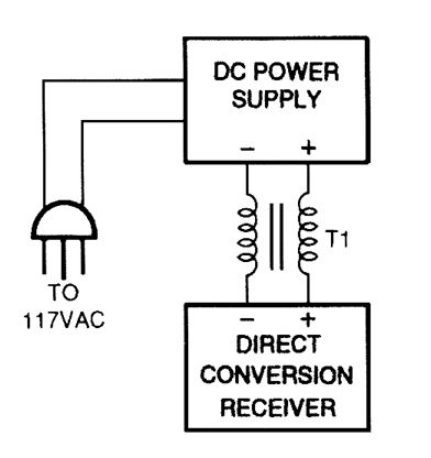


One cure for ac power line hum and ripple (caused by leakage current) is to use a well-regulated and filtered 9- to 18-Vdc power supply with a balancing choke (T1 in this illustration) between the power supply and the DCR. (View)
View full Circuit Diagram | Comments | Reading(1329)
The dual-channel photocoupler-optoisolator circuit
Published:2011/7/21 2:18:00 Author:Seven | Keyword: dual-channel, photocoupler-optoisolator
View full Circuit Diagram | Comments | Reading(758)
The circuit diagram of Led lattice electronic shielding controled by PLC
Published:2011/7/21 3:06:00 Author:Ecco | Keyword: PLC, Led dots electron shielding
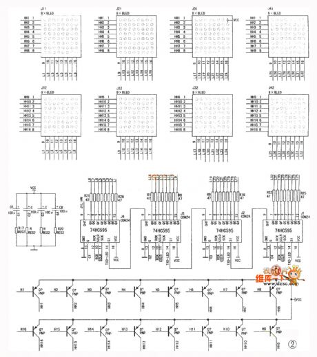
View full Circuit Diagram | Comments | Reading(873)
The dual-channel photocoupler-optoisolator anti-interference circuit
Published:2011/7/21 2:19:00 Author:Seven | Keyword: dual-channel, photocoupler-optoisolator, anti-interference
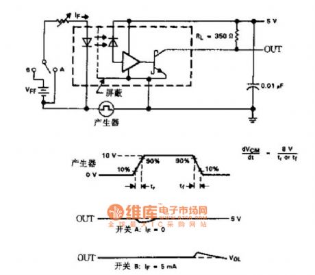
View full Circuit Diagram | Comments | Reading(976)
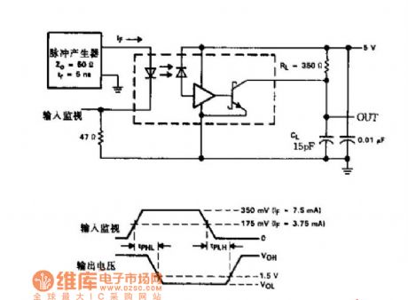
The photocoupler with load circuit
Published:2011/7/21 2:15:00 Author:Seven | Keyword: photocoupler
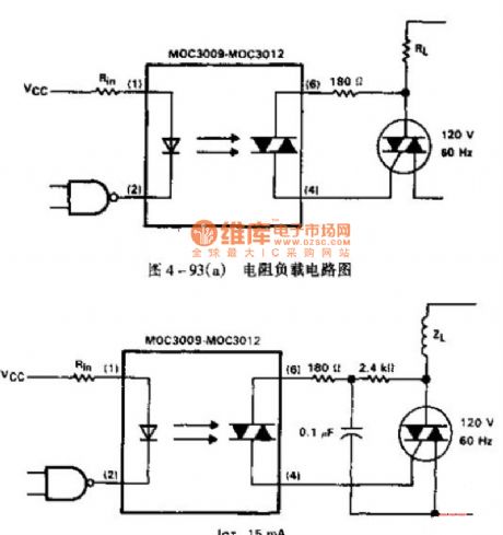
View full Circuit Diagram | Comments | Reading(929)
PRACTICAL_DIFFERENTIATOR
Published:2009/6/22 23:18:00 Author:Jessie

A differentiator has a high-pass charactenstic. Components are chosen by using the design equations. (View)
View full Circuit Diagram | Comments | Reading(1227)
The 3-terminal voltage stabilizer circuit
Published:2011/7/24 7:49:00 Author:Seven | Keyword: 3-terminal, voltage stabilizer

In the figure, resistor R1 provides bias current for the 3-terminal voltage stabilizer, and the need of R1<Veb2/Ib(max) must be met, if R1 is too high, the need in the above formula can't be met, the 3-terminal bias current is provided by base electricity of triode Tr2, and the output voltage is out of control.In figure 1, the output current of 0~5V is almost provided by Tr2, the power of Tr2 is large, so a radiator is needed.
A regulator diode can also form a simple regulator circuit, but the output current is only 10mA or so. (View)
View full Circuit Diagram | Comments | Reading(636)
CAPACITANCE_MULTIPLIER
Published:2009/6/22 23:17:00 Author:Jessie

View full Circuit Diagram | Comments | Reading(0)
PG_PASSWORD_PROTECTOR
Published:2009/6/22 23:01:00 Author:May

IC4, a static RAM, is mounted in a smart built-in switch over circuitry. This retains SRAM con-tents when power is off. The rest of the circuitry consists of address decoding logic and jumper JU1, used to decode a 16K address space for the 32K static RAM. Software is necessary and this is con-tained in the original article (see reference). (View)
View full Circuit Diagram | Comments | Reading(0)
ELECTRONIF_THERMOSTAT
Published:2009/6/22 23:16:00 Author:Jessie
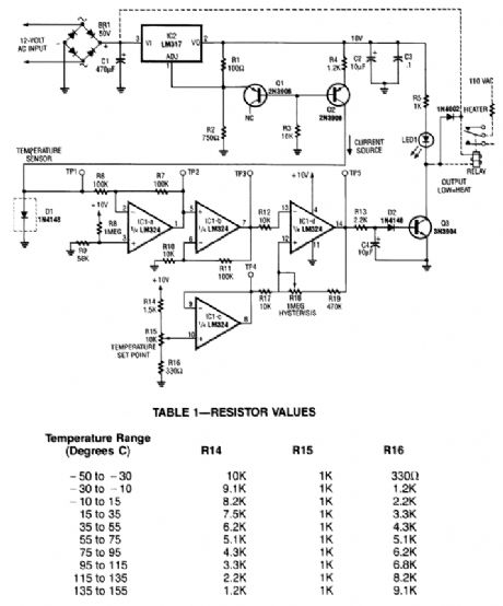
A diode, such as a IN4148, has a typical -2m V/℃ temperature coefficient at a 1 mA diode cur-rent. Q1 and Q2 form a constant current source. D1 is the temperature sensor. IC1-a and -b are dc amplifiers, with IC1-c a temperature reference voltage supply. IC1-d is a comparator with variable hysteresis. R14, R15, and R16 are chosen depending on the thermostat range desired. Q3 is a relay driver (2N3904). The relay used should handle the Ioad current or an optoisolator triac combination can be used. (View)
View full Circuit Diagram | Comments | Reading(3044)
TEMPERATURE_COMPENSATION_ADJUSTER
Published:2009/6/22 23:01:00 Author:May

The circuit shown delivers +10 to -10 mV°/C output using an Analog Devices' AD590 temperature transducer. Rx is a scaling resistor. (View)
View full Circuit Diagram | Comments | Reading(0)
PHASE_LOCKED_LOOP
Published:2009/6/22 23:15:00 Author:Jessie

The PLL will lock onto an input signal. Both triangle- and square-wave outputs are available.A quad op amp can be used in this circuit, which should be useful in the audio and LF radio region. (View)
View full Circuit Diagram | Comments | Reading(1791)
PHOTODIODE_LOG_CONVERTER_TRA_NSMITTER
Published:2009/6/22 23:00:00 Author:May


A logarithmic conversion is made on the output current of a photodiode to compress a fourdecade, light-intensity variation into a standard transmission range. The circuit is balanced at midrange, where R3 should be chosen so that the current through it equals the photodiode current. The log-conversion slope is temperature compensated with R6. Setting the reference output to 1.22 V gives a current through R2 that is proportional to absolute temperature because of D1 so that this level-shift voltage matches the temperature coefficient of R6. C1 has been added so that large-area photodiodes with high capacitance do not cause frequency instabilities. (View)
View full Circuit Diagram | Comments | Reading(0)
The reset stable amplifier(wave chopper amplifier) circuit
Published:2011/7/24 7:59:00 Author:Seven | Keyword: stable amplifier, wave chopper amplifier

The reset stable amplifier is one kind of wave chopper amplifier, whose circuit is shown in the figure, the amplifier works in the environment where the close loop gain is 1.The circuit can effectively remove the fault caused by offset voltage and bias current. The output of the circuit is a pulse whose amplitude is Vin. To understand its working principle, there is the need to analyse the circuit structure change when the switch S1 is pulled to different position. (View)
View full Circuit Diagram | Comments | Reading(509)
LOW_TEMPERATURE_SENSOR
Published:2009/6/22 23:13:00 Author:Jessie

A negative bias current can produce the off-set needed for below-zero readings using the LM34 or LM35 temperature sensor. (View)
View full Circuit Diagram | Comments | Reading(2520)
TEMPERATURE_SENSOR
Published:2009/6/22 23:09:00 Author:Jessie
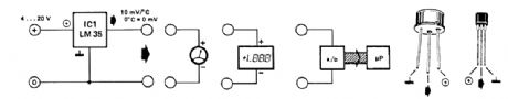
The LM35 temperature sensor provides an output of 10 mV/℃ for every degree Celsius over 0℃. At 20℃ the output voltage is 20 x 10 = 200 mV. The circuit consurnes 60 μA. The load resistance should not be less than 5 kΩ. A 4- to 20-V supply can be used. (View)
View full Circuit Diagram | Comments | Reading(2)
TELEPHONE_LINE_TESTER
Published:2009/6/22 22:59:00 Author:May

The telephone-line tester consists of nothing more than a meter (that's used to measure line voltage in the on- and off-hook state), three resistors (one of which is variable), a pushbutton switch, and a modular telephone connector. When the circuit is connected to the telephone line, a meter reading of 5 to 10 V (when S1 is pressed) indicates that the line is okay. (View)
View full Circuit Diagram | Comments | Reading(0)
| Pages:1387/2234 At 2013811382138313841385138613871388138913901391139213931394139513961397139813991400Under 20 |
Circuit Categories
power supply circuit
Amplifier Circuit
Basic Circuit
LED and Light Circuit
Sensor Circuit
Signal Processing
Electrical Equipment Circuit
Control Circuit
Remote Control Circuit
A/D-D/A Converter Circuit
Audio Circuit
Measuring and Test Circuit
Communication Circuit
Computer-Related Circuit
555 Circuit
Automotive Circuit
Repairing Circuit