
Circuit Diagram
Index 1383
WWV_CONVERTER
Published:2009/6/22 23:37:00 Author:May

This converter heterodynes the 15-MHz WWW signal with a 16-MHz oscillator so that it can be heard at 1 MHz on an ANI broadcast receiver. T1 and T2 are a modified 10.7-MHz IF transformer and AM BO oscillator coil, respectively. (View)
View full Circuit Diagram | Comments | Reading(0)
AUDIO_VOLUME_LIMITER
Published:2009/6/22 23:49:00 Author:Jessie

In this circuit,amplifier IC1-a provides signal amplification of 40 to+40 dB depending on thevalue of the LDR The LDR(ight dependent resistor)is driven by rectified audio from voltage follower IC1b and bridge rectifier D1 through D4 (View)
View full Circuit Diagram | Comments | Reading(0)
PSEUDOGROUND
Published:2009/6/22 23:37:00 Author:May
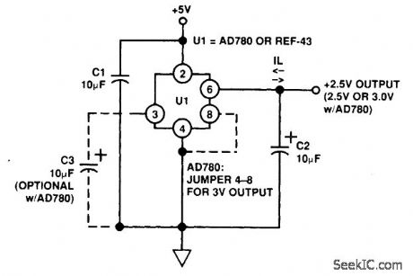
For op-amp circuits, a pseudo ground is often needed; a voltage reference IC can be used. The Analog Devices AD780 is used here for this application. This can sink or source current. (View)
View full Circuit Diagram | Comments | Reading(0)
BLOWN_FUSE_ALARM
Published:2009/6/22 23:49:00 Author:Jessie
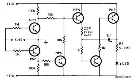
If the fuse blows, the LED indicator starts to blink. (View)
View full Circuit Diagram | Comments | Reading(1120)
LOW_FREQUENCY_ASTABLE
Published:2009/6/22 23:49:00 Author:Jessie


By using a high-gain low-current transistor, such as the 2N3565, a pair of Darlington-connected transistors (2N3565 and 2N3904) can be used in a high-impedance configuration. (View)
View full Circuit Diagram | Comments | Reading(1170)
SINGLE_CHIP_MESSAGE_SYSTEM
Published:2009/6/22 23:35:00 Author:May

The ISD1016 is a complete analog audio record/playback system on a chip. The analog signal is sampled and the samples stored in an EEPROM as analog levels. Upon playback, the analog data is read out and amplified. Up to 16 seconds of data(audio)can be stored. (View)
View full Circuit Diagram | Comments | Reading(0)
AUTOMOTIVE_BURGLAR_ALARM
Published:2009/6/22 23:35:00 Author:May

Alarm triggers on after a 13 second delay and stays on for 1-1 1/2 minutes. Then it resets automatically. It can also be turned off and reset by opening and reclosing S1. (View)
View full Circuit Diagram | Comments | Reading(0)
The low-noise and high-efficiency PWM step-down converting power supply circuit
Published:2011/7/24 3:29:00 Author:Seven | Keyword: low-noise, high-efficiency, power supply

In the figure is the adjustable step-down power supply which is based on the low-noise and high-efficiency PWM converter MAX887(8-SO package), and the external elements are few. The characters of it are: (1) the input voltage is from 3.5V to 11.5V, the output voltage is 1.25V to 10.25V; (2) the output current is 600mA, and the static current is 200μA, the standby mode is only 2.5μA; (3) the converting efficiency is 95%; (4) the fixed working frequency of MAX887 is 300KHZ, which effectively reduces the size and cost of the external element.
(View)
View full Circuit Diagram | Comments | Reading(546)
AUDIBLE_CONTINUITY_TESTER
Published:2009/6/22 23:35:00 Author:May

View full Circuit Diagram | Comments | Reading(0)
The +5V solid output step-down convert power supply circuit composed of MAX639
Published:2011/7/24 2:13:00 Author:Seven | Keyword: step-down, power supply

In the figure is the +5V solid output step-down convert power supply circuit composed of MAX639. MAX639 is a high-power step-down DC/AC converter. The input voltage ranges from 5.5V to 11.5V, the output is the +5V solid voltage or the adjustable voltage, the output current is 100mA, the converting efficiency is higher than 90%. The circuit has the function of low battery voltage detection and working/disable mode control.
(View)
View full Circuit Diagram | Comments | Reading(649)
CURRENT_REGULATOR_OP_AMP
Published:2009/6/22 23:35:00 Author:May
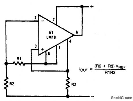
View full Circuit Diagram | Comments | Reading(647)
SIMPLE_AUDIO_VIDEO_CABLE_TESTER
Published:2009/6/22 23:34:00 Author:May

As simple as it looks, the audio/video cable tester tests cables while they are plugged in. You can flex them vigorously while listening to the built-in buzzer.Simply plug the ends of the cable in the appropriate jack. Only one end of the cable need be plugged in for a complete short test; the other end is left free. If the buzzer sounds, there is a short circuit somewhere in the cable. If nothing is heard, test for an intermittent short by flexing the cable several times, particularly in the plug area of both the free and plugged-in ends. (View)
View full Circuit Diagram | Comments | Reading(660)
SINGLE_SUPPLY_OP_AMP_APPLICATIONS
Published:2009/6/22 23:34:00 Author:May


An op amp that normally needs two supplies can be used when only a single supply is needed. The value of V+ should be twice the minimum allowable values of the positive and negative voltages normally needed. For example, a 12-V single-supply application would require an op amp capable of ±6-V operation. (View)
View full Circuit Diagram | Comments | Reading(1823)
The 20W switch DC voltage stabilizing power supply circuit
Published:2011/7/24 2:05:00 Author:Seven | Keyword: DC voltage, power supply
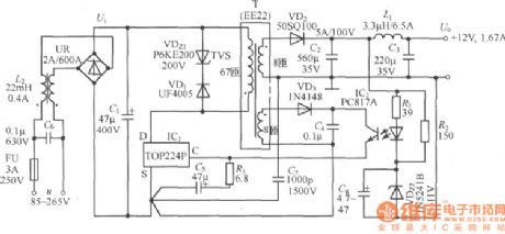
The technique indicators of the power supply are shown as follows:AC input voltage range: u=85~265V; input grid frequency: fLl=47~440Hz; Output voltage (Io=1.67A): Uo=12V;MAX output power: IOM=1.67A; Continuous output power: Po=20W(TA=25℃ or 15W(TA=50℃);Voltage adjusting ratio: η=78%; Output wave voltage MAX value: ±60mV; Working temperature range: TA=0~50℃.
(View)
View full Circuit Diagram | Comments | Reading(817)
ADJUSTABLE_CONTINUITY_TESTER
Published:2009/6/22 23:34:00 Author:May

A problem with most continuity testers is that the exact decision point (circuit resistance) be-tween continuity and open is indefinite. This circuit allows setting of this point to a known resistance between 1 and 50Ω. (View)
View full Circuit Diagram | Comments | Reading(926)
VOCAL_STRIPPER_POWER_SUPPLY
Published:2009/6/22 23:33:00 Author:May

The power supply schematic for the lead vocal filter circuit. (View)
View full Circuit Diagram | Comments | Reading(564)
SHORT_CIRCUIT_BEEPER
Published:2009/6/22 23:33:00 Author:May


This design offers a way to trace resistance in the milliohm range, right to a short between bridged traces beneath a solder mask. It simply translates resistance into an audible tone, which in-creases in pitch as the measured value approaches zero.In the classic op-amp multivibrator (shown in the inset), oscillation frequency is determined not only by the R1/C1 time constant, but also by the hysteresis set by the R2/R3 resistance ratio. Al in the main figure, with current boosters Q1 and Q2, is this same configuration.Assuming a virtual ground at the output of A2, free-run frequency is about 1 kHz-quite audible through a tiny 8-Ω speaker. Q1 and Q2 deliver a ±10-V squarewave to R4, dumping a ±100 mA through a short circuit placed across the probe tips. R5 ensures that open circuit voltage never ex-ceeds ±0.1 V.AZ monitors the voltage between the probes. The differential input must have its own separate path to the probe tips to eliminate test lead resistance from the measurement. Miniature zip-cord sold as loudspeaker wire makes a tidy two-conductor test lead.When the probes are open, A2's gain equals the R4/R5 divider loss, and the output of both am-plifiers is identical. This has two effects: first, hysteresis is greatly increased and the frequency falls to a low growl; second, the loudspeaker that bridges the two in-phase outputs is effectively silenced.The dead short across the probe tips will return nothing to AZ and the circuit will squeal at its nominal 1-kHz rate. Anything less than a perfect short produces some output from A2, increasing multivibrator hysteresis and lowering the pitch. The circuit has so much 'leverage, and the ear is so sensitive to pitch changes in this range, that it's easy to resolve minute resistance differences.Any general-purpose op amp will suffice in this circuit-a couple of 741s or an equivalent dual. (View)
View full Circuit Diagram | Comments | Reading(796)
PARALLELED_POWER_OP_AMPS
Published:2009/6/22 23:30:00 Author:May
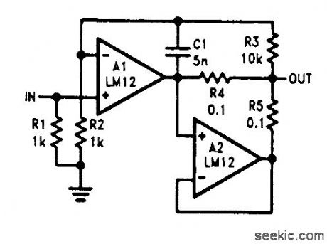
Two power op amps can be paralleled using this master/slave arrangement, but high-requency performance suffers. (View)
View full Circuit Diagram | Comments | Reading(536)
VOCAL_STRIPPER
Published:2009/6/22 23:29:00 Author:May

The schematic of the lead vocal filter is shown in the figure. The left and right channel signals are coupled through C1 and'C2 to buffer amps IC4-a and IC4-b. From the buffer amps, the left and right channel signals pass through active crossovers IC5-a and IC5-b, sending all low frequencies to a final mixer IC6-c, and all middle and high frequencies to analog delay lines IC1 and IC2, RD5106256-sam-ple bucket-brigades. Integrated circuit IC2 delays the left-channel signal by 2.4 ms, set by the fixed-frequency clock generated by 1/2IC3, R47, and C24. The right channel signal is delayed by IC1 with a variable-frequency clock generated by 1/2IC3, R48, R49, and C23. Potentiometer R49 is used for phase adjustment.The output of each delay line from IC1 and IC2 passes through low-pass filters IC6-a and -d, and their associated parts, to filter out high-frequency sample-steps produced by IC1 and IC2. Balance control R36 is adjusted for equal amplitude of the left and right channels. ICG-b is a difference am-plifier that cancels all lead vocals that are common to both channels. The resulting signal from ICG-b is remixed with low frequencies by ICG-c and is then sbnt to the output via buffers IC4-c and IC4-d. (View)
View full Circuit Diagram | Comments | Reading(0)
ENHANCED_OP_AMP_BALANCED_AMPLIFIER
Published:2009/6/22 23:29:00 Author:May

The classic single op-amp balanced circuit works well in low-source-impedartce configurations, but tends to struggle in higher-source-imp edance applications because of the varying input impedance of the inputs referred to ground.
A modified version of the classic op-amp configuration of the figure uses a different set of formulas to determine the resistor values. It equalizes the impedance of both inputs by considering the op amp's active participation. (View)
View full Circuit Diagram | Comments | Reading(2684)
| Pages:1383/2234 At 2013811382138313841385138613871388138913901391139213931394139513961397139813991400Under 20 |
Circuit Categories
power supply circuit
Amplifier Circuit
Basic Circuit
LED and Light Circuit
Sensor Circuit
Signal Processing
Electrical Equipment Circuit
Control Circuit
Remote Control Circuit
A/D-D/A Converter Circuit
Audio Circuit
Measuring and Test Circuit
Communication Circuit
Computer-Related Circuit
555 Circuit
Automotive Circuit
Repairing Circuit