
Circuit Diagram
Index 1390
SET_TIME_WINDOWS_WITHIN_A_CLOCK
Published:2009/6/22 22:49:00 Author:May

At times, it is necessary to produce pulses of adjustable width and whose start times might vaty with reference to a master clock. The input signal is inverted and buffered by U1A, while U1B and U1C reinvert the signal to produce square, buffered renditions of the input signal. Potentiometers R3 and R4 set references for the comparators.The input polarity of U2A keeps its output transistor tumed on until the voltage at the nonin-verting input exceeds the reference set by R4 (the rising edge adjustment). When this reference voltage is exceeded, the output transistor is turned off and the output signal is pulled up via R6.Meanwhile, the input polarity of U2B keeps its output transistor turned off until the voltage at the in-verting input exceeds the reference set by R3 (the falling edge adjustment). When this reference voltage is surpassed, the output transistor of U2B is turned on, pulling the output signal low through the wired-OR conftguration of U2. The output of U2 is then double-inverted and buffered by U1D and U1E. What results is a pulse whose start time (rising edge) can be adjusted by R4, and whose stop time (falling edge) can be adjusted by R3.The output of the comparators is pulled up to the input waveform through resistor R6 to U1C.This prevents the comparators from switching during the low cycle of the input waveform, regard-less of the positions of R3 and R4. This has the effect of locking out changes during the low period of the input signal, and would probably require additional logic if it were done strictly in the digital domain.The circuit, with the component values shown, works well between about 50 and 150 kHz. (View)
View full Circuit Diagram | Comments | Reading(0)
PROGRAMMABLE_RESISTOR_CIRCUIT
Published:2009/6/22 22:49:00 Author:May

IC1 CD4066 quad bilateral switchC1 0.1-μF capacitorRI 10-kΩ, 1/4-W 5% resistorR2 4.7-kΩ, 1/4-W 5% resistorR3 2.2-kΩ, 1/4-W 5% resistorR4 1-kΩ, 1/4-W 5% resistorR5 1-MΩ, 1/4-W 5% resistor
A programmable resistor can replace a potentiometer or fixed resistor. Remember that the ON resistance of IC1 might have to be taken into account in some applications. (View)
View full Circuit Diagram | Comments | Reading(0)
PROGRAMMABLE_RESISTOR_CIRCUIT
Published:2009/6/22 22:49:00 Author:Jessie
IC1 CD4066 quad bilateral switchC1 0.1-μF capacitorRI 10-kΩ, 1/4-W 5% resistorR2 4.7-kΩ, 1/4-W 5% resistorR3 2.2-kΩ, 1/4-W 5% resistorR4 1-kΩ, 1/4-W 5% resistorR5 1-MΩ, 1/4-W 5% resistor
A programmable resistor can replace a potentiometer or fixed resistor. Remember that the ON resistance of IC1 might have to be taken into account in some applications. (View)
View full Circuit Diagram | Comments | Reading(2405)
ALARM_DIALER
Published:2009/6/22 22:48:00 Author:May


This circuit dials a stored DTMF tone sequence from EPROM when a control line is taken to 0 V. IC1 is a Schmitt trigger oscillator, running at around 2 Hz. It clocks a 4024 binary counter. The coun-ter's outputs connect to the address leads of the EPROM. A 2716 was used here, but the choice of EPROM is by no means critical.Normally, the counter is held reset by a logic 1 on its reset pin (pin 2). When the trigger input is sent low, pin 10 of IC1 goes low, pin 3 goes high, and the reset is removed from the counter. It then begins to clock, incrementing the EPROM. When moved from address 000000, the data on bit DO of the EPROM changes to a logic 1 and holds the circuit running. The last address should have data 11111110 to reset the circuit to standby. (View)
View full Circuit Diagram | Comments | Reading(0)
BUFFER_FOR_A_D_CONVERTERS
Published:2009/6/22 22:47:00 Author:May

This circuit uses an LT1366 driving an LTC1288 two-channel micropower A/D. The LTC1288 can accommodate voltage references and input signals equal to the supply rails. The sampling nature of this A/D eliminates the need for an external sample-and-hold, but might call for a drive amplifier be-cause of the A/D's 12-ps settling requirement. The LT1366's rail-to-rail operation and low-input off-set voltage make it well suited for low-power, low-frequency A/D applications. In addition, the op-amp's output settles to 1% in response to a 3-mA load step through 100 pF in less than 1.5μs. (View)
View full Circuit Diagram | Comments | Reading(0)
SELF_RETRIGGERING_TIMED_ON_GENERATOR
Published:2009/6/22 22:47:00 Author:May
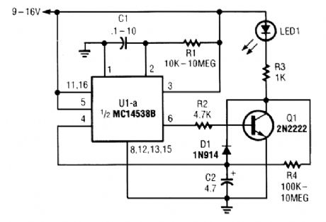
When power is first applied to the circuit, CZ begins to charge via LED1, R3, and R4. When the voltage across C2 reaches UI's input trigger level, the output of UI at pin 6 goes positive for a period that is determined by the values of C1 and R1. That turns Q1 on, discharging C2 through Dl and Q1.
At the end of the set period, the output of UI at pin 6 goes low, turning Q1 off and allowing the current to begin flowing through LED1, R3, and R4 to gain charge C2, causing the cycle to repeat.The repeat time is determined by the values of R3, R4, and C2. The previous formula won't be as accurate for this circuit, but it will at least get you close enough for the capacitor value; then R4, can be fine-tuned to obtain the desired timing period. (View)
View full Circuit Diagram | Comments | Reading(0)
PROGRAMMABLE_LIGHT_ACTIVATED_RELAY
Published:2009/6/22 22:47:00 Author:May

Digital inputs A, B, C, D select different light levels by varying the value of bridge circuit resis-tance R4.IC1 741 op ampIC2 CD4066 quad bilateral switchQ1 NPN transistor (2N2222, 2N3904, or similar) D1 diode (1N4002, or similar)C1 0.1-μF capacitorR1 photoresistorR2, R3 390-kΩ, 1/4-W 5% resistorR4, R5 1-MΩ, 1/4-W 5% resistorR6 820-kΩ, 1/4-W 5% resistorR7 470-kΩ, 1/4-W 5% resistorR8 270-kΩ, 1/4-W 5% resistorR9 100-kΩ, 1/4-W 5% resistorK1 relay to suit load (View)
View full Circuit Diagram | Comments | Reading(0)
TRAFFIC_LIGHT_CONTROLLER
Published:2009/6/22 22:49:00 Author:Jessie

Oscillator U5A-B drives a 4017 divide-by-10 counter. The first output of U1 appears at pin 3, which supplies a positive voltage to U2, a MOO 3010 optocoupler/triac-driver IC, turning it and triac TR1 on. That lights I1, the red lamp. The second output appears at pin 2 and passes through D1 to the second MOC 3010, U3, thereby lighting the yellow lamp, I2. The third output at pin 4 turns on UJ4 and the green lamp, I3. The fourth output at pin 7 travels through D2 and into U3 to light the yellow lamp, I2, again.If you would like the traffic-light system to follow the normal sequence of green, yellow, and red, make the following circuit changes: Disconnect pins 10 and 15 of U1 from each other. Remove D1 and D2 and connect pin 2 of U1 to pin 1 of U3. Then connect pins 7 and pins 15 of UI together. Use U2 to drive I3 (the green light) and U4 for I1 (the red light). (View)
View full Circuit Diagram | Comments | Reading(3826)
ALARM_DIALER
Published:2009/6/22 22:48:00 Author:Jessie
This circuit dials a stored DTMF tone sequence from EPROM when a control line is taken to 0 V. IC1 is a Schmitt trigger oscillator, running at around 2 Hz. It clocks a 4024 binary counter. The coun-ter's outputs connect to the address leads of the EPROM. A 2716 was used here, but the choice of EPROM is by no means critical.Normally, the counter is held reset by a logic 1 on its reset pin (pin 2). When the trigger input is sent low, pin 10 of IC1 goes low, pin 3 goes high, and the reset is removed from the counter. It then begins to clock, incrementing the EPROM. When moved from address 000000, the data on bit DO of the EPROM changes to a logic 1 and holds the circuit running. The last address should have data 11111110 to reset the circuit to standby. (View)
View full Circuit Diagram | Comments | Reading(3502)
BUFFER_FOR_A_D_CONVERTERS
Published:2009/6/22 22:47:00 Author:Jessie
This circuit uses an LT1366 driving an LTC1288 two-channel micropower A/D. The LTC1288 can accommodate voltage references and input signals equal to the supply rails. The sampling nature of this A/D eliminates the need for an external sample-and-hold, but might call for a drive amplifier be-cause of the A/D's 12-ps settling requirement. The LT1366's rail-to-rail operation and low-input off-set voltage make it well suited for low-power, low-frequency A/D applications. In addition, the op-amp's output settles to 1% in response to a 3-mA load step through 100 pF in less than 1.5μs. (View)
View full Circuit Diagram | Comments | Reading(1587)
SELF_RETRIGGERING_TIMED_ON_GENERATOR
Published:2009/6/22 22:47:00 Author:Jessie
When power is first applied to the circuit, CZ begins to charge via LED1, R3, and R4. When the voltage across C2 reaches UI's input trigger level, the output of UI at pin 6 goes positive for a period that is determined by the values of C1 and R1. That turns Q1 on, discharging C2 through Dl and Q1.
At the end of the set period, the output of UI at pin 6 goes low, turning Q1 off and allowing the current to begin flowing through LED1, R3, and R4 to gain charge C2, causing the cycle to repeat.The repeat time is determined by the values of R3, R4, and C2. The previous formula won't be as accurate for this circuit, but it will at least get you close enough for the capacitor value; then R4, can be fine-tuned to obtain the desired timing period. (View)
View full Circuit Diagram | Comments | Reading(1379)
PROGRAMMABLE_LIGHT_ACTIVATED_RELAY
Published:2009/6/22 22:47:00 Author:Jessie
Digital inputs A, B, C, D select different light levels by varying the value of bridge circuit resis-tance R4.IC1 741 op ampIC2 CD4066 quad bilateral switchQ1 NPN transistor (2N2222, 2N3904, or similar) D1 diode (1N4002, or similar)C1 0.1-μF capacitorR1 photoresistorR2, R3 390-kΩ, 1/4-W 5% resistorR4, R5 1-MΩ, 1/4-W 5% resistorR6 820-kΩ, 1/4-W 5% resistorR7 470-kΩ, 1/4-W 5% resistorR8 270-kΩ, 1/4-W 5% resistorR9 100-kΩ, 1/4-W 5% resistorK1 relay to suit load (View)
View full Circuit Diagram | Comments | Reading(1867)
SIMPLE_BIDIRECTIONAL_BUFFER_DESIGN
Published:2009/6/22 22:47:00 Author:Jessie

This circuit shown in the figure uses two 74LS241s. When both input/output lines are high, IC-1A and IC-2B turn on, and C1 and CZ are charged to high voltage. Meanwhile, IC-1B and IC-2A are off to prevent a logic 1 latch. (View)
View full Circuit Diagram | Comments | Reading(1248)
VOLTAGE_FOLLOWER
Published:2009/6/22 22:46:00 Author:Jessie
View full Circuit Diagram | Comments | Reading(127)
DARKNESS_MONITOR
Published:2009/6/22 22:45:00 Author:Jessie

When light strikes detector Q1,Q2 is cut off,allowing bias to reach SCR1,triggering SCR1 and lighting LED1,S1 resets the circuit. (View)
View full Circuit Diagram | Comments | Reading(743)
5_V_DIAL_TONE_CIRCUIT
Published:2009/6/22 22:45:00 Author:May

This circuit uses inexpensive, common components to generate a precise dial tone for phone applications (see the figure). U1 (an Intel 82C54 timer-counter) generates 350- and 440-Hz square waves that are filtered by R1/C1 and R3/C2, and mixed together by resistors R2 and R4.An operational amplifier configured as a 395-Hz, Sallen-Key, second-order bandpass filter (halfway between 350 and 440 Hz) removes unwanted signal harmonics. Almost any timer-counter can be used as the signal source, so long as it produces roughly square-wave outputs. (View)
View full Circuit Diagram | Comments | Reading(1727)
LIGHT_CONTROLLED_MONOSTABLE
Published:2009/6/22 22:44:00 Author:May
The light-controlled monostable was produced by combining a 555 monostable multivibrator with a pair of light-controlled comparators. The circuit can be used to enable the operation of the load device, depending on the time of day. During the daylight hours, the timer U2, is disabled, and so produces no output. However, during the nighttime hours, U2 is enabled by the output of UI-b so that pressing S1 initiates a timing cycle, which activates LED1 for a time determined by R8 and C1. (View)
View full Circuit Diagram | Comments | Reading(1076)
ANALOG_NONINVERTING_SWITCHED_BUFFER
Published:2009/6/22 22:44:00 Author:May

Here is noninverting solution. (View)
View full Circuit Diagram | Comments | Reading(490)
SINGLE_SUPPLY_ac_BUFFER_AMPLIFIER
Published:2009/6/22 22:44:00 Author:May
This buffer Right be used with a single sup-ply without special considerations. The input is dc biased to mid-operating point and is ac cou-pled. Its input impedance is approximately 500 kΩ at low frequencies. Note that for dc loads ref-erenced to ground, this quiescent current is in-creased by the load current set at the input dc bias voltage. (View)
View full Circuit Diagram | Comments | Reading(1071)
SINGLE_SUPPLY_PHOTODIODE_AMPLIFIER
Published:2009/6/22 22:44:00 Author:May
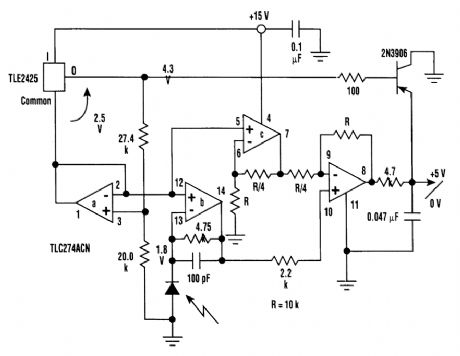
This circuit provides a reverse-bias operating point and output voltage offset and uses a single-polarity power supply. The floating reference voltage from TLE2425 serves to bias the diode in a reverse-polarity mode. It also provides a clamping level at the output. Consequently, linear response to illumination is maintained for a 5-V range from dark current to full sunlight conditions. (View)
View full Circuit Diagram | Comments | Reading(1396)
| Pages:1390/2234 At 2013811382138313841385138613871388138913901391139213931394139513961397139813991400Under 20 |
Circuit Categories
power supply circuit
Amplifier Circuit
Basic Circuit
LED and Light Circuit
Sensor Circuit
Signal Processing
Electrical Equipment Circuit
Control Circuit
Remote Control Circuit
A/D-D/A Converter Circuit
Audio Circuit
Measuring and Test Circuit
Communication Circuit
Computer-Related Circuit
555 Circuit
Automotive Circuit
Repairing Circuit