
Circuit Diagram
Index 1389
SOLAR_POWER_SUPPLY_WITH_LINEAR_REGULATOR
Published:2009/6/22 22:58:00 Author:Jessie

This regulator delivers a constant 2.4 Vdc for powering small devices that run on two AA cells, such as cassettes and small radios. Regulator drop is about 0.3 volt. This should be considered when choosing solar cells. Load current is typically 125 mA. (View)
View full Circuit Diagram | Comments | Reading(0)
TELEPHONE_HOLD_CIRCUIT
Published:2009/6/22 22:57:00 Author:Jessie

When S1 is pressed, the SCR fires, and places LED1 and R1 across the phone line. The line volt-age drops to about 20 V, which holds the connec-tion to the phone company's central office. (View)
View full Circuit Diagram | Comments | Reading(1334)
FCC_PART_68_PHONE_INTERFACE
Published:2009/6/22 22:56:00 Author:May

An FCC Part 68 interface is required any time you connect any circut of your own to the phone line. (View)
View full Circuit Diagram | Comments | Reading(660)
The 555 linear voltage/frequency converter circuit
Published:2011/7/20 7:37:00 Author:Seven | Keyword: voltage/frequency converter

See as figure 5-34, the linear voltage/frequency converter consists of a differentiation/integration circuit and a single stable trigger delay circuit, which is used in voltage/frequency conversion. The IC is a MOSFET computing amplifier CA3140(OR 4573), which forms the integration circuit of the differentiation input, its output terminal control is added to the trigger of IC2, the output of the single stable trigger circuit is added to the non-inverting terminal of the integrator, by changing the integral phase, the output of IC1, a triangular wave, increases or decreases in linearity.
(View)
View full Circuit Diagram | Comments | Reading(2760)
VISUAL_METRONOME
Published:2009/6/22 22:55:00 Author:May
View full Circuit Diagram | Comments | Reading(514)
LED_LIGHTWAVE_COMMUNICATIONS_TRANSMITTER
Published:2009/6/22 22:55:00 Author:May

View full Circuit Diagram | Comments | Reading(859)
The automatic control circuit diagram of vestibular light with photocoupler
Published:2011/3/30 22:53:00 Author:Ecco | Keyword: automatic control, vestibular light , photocoupler
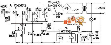
According to the circuitry, A stands for four sets of analog electronic switches(S1~S4: the parallel connection of S1,S2,S3 is used as time-delay circuit, which could increase the driving power and anti-interference capability. When they are connected to the power, and they could control vestibular light H directly by bidirectional triode thyristor VT with driving of R4,B6; S4 and light dependent resistor Rl. etc composed environmental light measuring circuitry. When the door is closed, the reed KD in the door will influenced by magnet, its contacts will be disconnected, and S1, S2, S3 are in the state of ON . When in the night, the host come back and open the door, the magnet will separated from KD, and the contacts will be connected. At the same time, the 9V supply will charge C1 by passing R1, the voltage in two terminals rise to 9V quickly, and commutating voltage passes S1,S2,S3 and R4 to make B6 lighted and bidirectional triode thyristor breakovered. H is lit. That is torealize automatic control. When the door in closed, the magnet will make the contacts of KD disconnected, and 9v supply will stop charging for C1, the circuitry is in the time-delay state. C1 begin discharges to the R3, after a period of time delay, the two terminal voltage of C1 will lower than opening voltage(1.5V) of S1,S2,S3, and they will recover the disconnected state, and B6 and H stop working. That is to realize the function of turning off a lamp while postponing.
(View)
View full Circuit Diagram | Comments | Reading(622)
PRINTER_PORT
Published:2009/6/22 22:55:00 Author:May


A 16-step programmable current generator can be modified so that it's controllable by a printer port. This is done by switching the resistor connected between the output of the generator's OA1 op amp and the input of OA2. The CMOS single 16-channel analog multiplexer (ICl) chooses one resis-tor at a time, in accordance with the code sent by the printer port through four of its eight data-out-put lines (pins 2 to 9). In addition, one control line (pin 1) is used to enable the operation. As a result, 16 outputs can be selected by a 4-bit word (the table shows the relationship between data word and selected resistor).The following must be fulfilled in order for the circuit to work as a true current generator:
R2×Rd-Rb×Rc =0
The smaller the resistors' tolerance (especially RI through R16), the greater the output resis-tance of the generator.Because the OA2 is connected as a repeater, the current I2 = O, and only the load current flows through one of the RI through R16 resistors. Therefore:
where Vout=Vin;X=1…16;and Ron≤150Ω(for VDD=10 V) is the resistance of one analog switch(CD4067)in conduction Therefore,the values of resistors R1 through R16 can be inferred from the needed currents∶
The Turbo c++ program also controls the current through the load
(View)
View full Circuit Diagram | Comments | Reading(1298)
The 555 quadruple frequency multiply circuit
Published:2011/7/20 7:28:00 Author:Seven | Keyword: quadruple frequency, multiply circuit
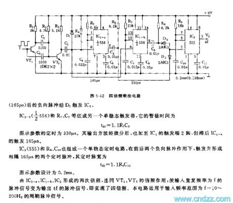
This multiply circuit can convert the period sequence of f1 into output pulse signal of f0=4f1, which is a quadruple frequency circuit, see as figure 5-42. The circuit includes the differentiation twice frequency circuit, single stable timing circuit and double frequency circuit and so on. VT1, R1, C1, C2 and R2 compose the phase inverting amplifier and differentiation circuit. C2, R2 and C1, R2 compose the differentiation circuit which forms 2 undershoot narrowing pulses, the first doubling is done at the collecting electrode of VT2.
(View)
View full Circuit Diagram | Comments | Reading(614)
AUDIBLE_METRONOME
Published:2009/6/22 22:54:00 Author:May
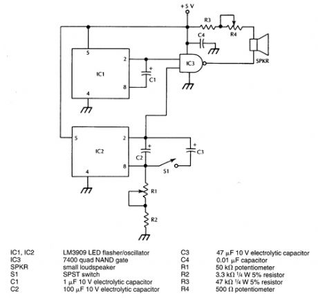
IC1 generates an audible frequency while a variable very low frequency is generated by IC2. R1 sets the metronome rate. The two signals are combined in IC3. (View)
View full Circuit Diagram | Comments | Reading(596)
CALLER_ID_CIRCUIT
Published:2009/6/22 22:54:00 Author:May

This caller ID circuit uses the Motorola MC145447 IC chip. This servlce must be available from your local phone company In order for this circuit to be used. (View)
View full Circuit Diagram | Comments | Reading(5035)
EIGHT_DECADE_LIGHT_METER
Published:2009/6/22 22:54:00 Author:May

A logarithmic amplifier is adapted to a battery-powered light meter. An LM10, combined op amp and reference, is used for the second amplifier and to provide the regulated voltage for offsetting the logging circuit and powering the bias-current compensation. This can provide input current resolution ofbetter than ±2 pA over 15 to 55℃. Because a meter is the output indicator, there is no need to optimize frequency compensation. Low-cost single transistors are used for logging because the temperature range is limited. The meter is protected from overloads by clamp diodes D2 and D3.Silicon photodiodes are more sensitive to infrared than visible light, so an appropriate filter must be used for photography. Alternately, gallium-ars enide-phosphide diodes with suppressed IR response are becoming available. (View)
View full Circuit Diagram | Comments | Reading(1030)
TELEPHONE_AUDIO_INTERFACE
Published:2009/6/22 22:52:00 Author:May

Used to record and play back tapes vla the phone lines,this simple circuit has an audio level switch (S1). (View)
View full Circuit Diagram | Comments | Reading(0)
COLORIMETER
Published:2009/6/22 22:52:00 Author:May
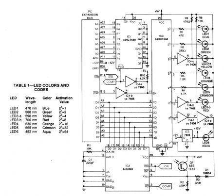
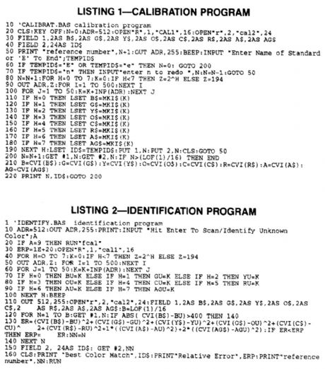
A hardware/software combination activates In turn,one of several LEDs enuts a portion of the visible spectrum .A phototransistor measures the light reflected by the surface being measured,andan 8-bit analog-to-digital converter(ADC) translates the phototransistor’s output into a digital format that the computer can interpret Seven LEDs (blue,aqua,green,yellow,orange,crimson,and red) provride a range of readings across the visible spectrum Lack of spectral continuity among adjacent LED colors could skew results,so the circuit provides built-in compensation for this error.
Two simple BASIC programs control the circuit’s operation. One allows you to define a set of standards by measunng known Color samples and recording the values with an associated name The other program measures unknown samples and provides the best match with the defined standards,as well as a relative error factor. (View)
View full Circuit Diagram | Comments | Reading(3221)
RS_422_TO_RS_232_CONVERTER
Published:2009/6/22 22:52:00 Author:May

The circuit supplies two LEDs for visual indication of line activity and terminating resistors when needed. The 220-Q resis-tors and 5-V zeners at the RS-422 line inputs supply circuit protection.Switch SW7 allows the circuit monitor both transmitted and received signals when tee-connected into an RS-232 line. One function of this optional feature is the ability to test a software-locking device that connects to the COM1 port on an IBM PC. (View)
View full Circuit Diagram | Comments | Reading(2989)
SET_TIME_WINDOWS_WITHIN_A_CLOCK
Published:2009/6/22 22:49:00 Author:Jessie

At times, it is necessary to produce pulses of adjustable width and whose start times might vaty with reference to a master clock. The input signal is inverted and buffered by U1A, while U1B and U1C reinvert the signal to produce square, buffered renditions of the input signal. Potentiometers R3 and R4 set references for the comparators.The input polarity of U2A keeps its output transistor tumed on until the voltage at the nonin-verting input exceeds the reference set by R4 (the rising edge adjustment). When this reference voltage is exceeded, the output transistor is turned off and the output signal is pulled up via R6.Meanwhile, the input polarity of U2B keeps its output transistor turned off until the voltage at the in-verting input exceeds the reference set by R3 (the falling edge adjustment). When this reference voltage is surpassed, the output transistor of U2B is turned on, pulling the output signal low through the wired-OR conftguration of U2. The output of U2 is then double-inverted and buffered by U1D and U1E. What results is a pulse whose start time (rising edge) can be adjusted by R4, and whose stop time (falling edge) can be adjusted by R3.The output of the comparators is pulled up to the input waveform through resistor R6 to U1C.This prevents the comparators from switching during the low cycle of the input waveform, regard-less of the positions of R3 and R4. This has the effect of locking out changes during the low period of the input signal, and would probably require additional logic if it were done strictly in the digital domain.The circuit, with the component values shown, works well between about 50 and 150 kHz. (View)
View full Circuit Diagram | Comments | Reading(1097)
555 as the D power amplifier circuit
Published:2011/7/20 7:16:00 Author:Seven | Keyword: power amplifier

See as figure 5-44, IC(555), R1, R2 and C1 compose a controllable multi-resonance oscillator whose frequency is 100KHz, duty cycle is 50%. The control terminal 5-pin is added with an audio signal, then the output of 3-pin is a PWM pulse signal whose PWM is in forward proportion to the amplitude. After filtering by L and C3, an amplified audio signal is got.
(View)
View full Circuit Diagram | Comments | Reading(2306)
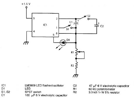
LOW_FREQUENCY_CLOCK
Published:2009/6/22 22:50:00 Author:May

The LM3090 is an LED flasher IC that is designed to oscillate at low frequencies. The clock out-put of the first circuit can be changed by changing the value of the capacitor, and the second circuit lets you adjust the frequency with the trimmer. BI can be one or two alkaline 1.5-V cells. The LM3909 can supply up to 45-mA pulses at greater than 2V. (View)
View full Circuit Diagram | Comments | Reading(799)
The 555 dual electric door bell circuit (1)
Published:2011/7/20 7:58:00 Author:Seven | Keyword: electric door bell
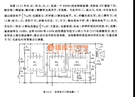
See as figure 15-27, IC1, R1, R2 and C1 compose a 800Hz audio oscillator circuit, when AN is pressed, the 2-pin of the trigger is connected with the earth, the 3-pin of the output terminal is reversed to be in a high LEV and starting to oscillate. Meanwhile, C1 is charged by R2, when the charge voltage is over the threshold LEV of 2/3VDD, the circuit is reset and stopping oscillating, the 3-pin is in a low LEV. The output of IC1 is sent to the 2-pin of IC2 and 13-pin of IC3, which makes IC2 and IC3 to be controlled by the output state of IC1.
(View)
View full Circuit Diagram | Comments | Reading(806)
FREQUENCY_DIVIDER_FOR_MEASUREMENTS
Published:2009/6/22 22:49:00 Author:May

This circuit is meant to be driven by a 1-MHz standard signal of a few volts amplitude. U1 through U5 are 7490 decade counter/divider and produce a division ratio of 100,000:1. Successive divisions of 10 can be tapped off, if desired, between stages. One or more stages can be added for still lower frequencies. (View)
View full Circuit Diagram | Comments | Reading(1739)
| Pages:1389/2234 At 2013811382138313841385138613871388138913901391139213931394139513961397139813991400Under 20 |
Circuit Categories
power supply circuit
Amplifier Circuit
Basic Circuit
LED and Light Circuit
Sensor Circuit
Signal Processing
Electrical Equipment Circuit
Control Circuit
Remote Control Circuit
A/D-D/A Converter Circuit
Audio Circuit
Measuring and Test Circuit
Communication Circuit
Computer-Related Circuit
555 Circuit
Automotive Circuit
Repairing Circuit