Amplifier Circuit
Op amp application input end zeroing circuit diagram 1
Published:2011/5/16 21:52:00 Author:Rebekka | Keyword: Op amp application , input end zeroing | From:SeekIC

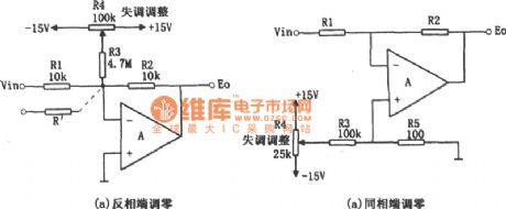
Figure (a) is a relatively simple circuit. It uses the input resistors R1 and the feedback resistor R2 as a part of the attenuation network. It generates a variable offset voltage with resistor R3 at the inverting input end. The voltage of the circuit is divided by R3 and R1,R2. The 2 ends of the potentiometer R4 connect with ± 15V power supply. The partial pressure ratio is about 1000 / 1. It can get ± 15mV offset voltage range. In figure (a), the general formula of the offset voltage adjustment range is:
Offset voltage range = ± VD · [(R1 ∥ R2) / R3] (± VD = ± 15V)
When there are multiple input signals at the reverse side. It is shown in figure (a) by the virtual display line. Its offset voltage range: Multiple input offset voltage range = ± VD [(R1 ∥ R2 ∥ Rl ') / R3] (± VD = ± l5V).
The circuit shown in figure (b) has a large application value. Since the adjusting voltage has no relationship with the feedback components, while the adjusting voltage is applied to the phase input terminal and avoid the winning stream signaling pathways. In this circuit, the resistance value of R3 and R5(100kΩ, 100Ω) form the 1000 / I voltage dividing circuit. The 2 terminals of R5 get ± 15mV offset voltage adjustment range. When the values of R3, R5 change. The offset voltage adjustment range is determined by:
Offset voltage adjustment range = ± VD · (R5/R3) (± VD = ± l5V)
Reprinted Url Of This Article:
http://www.seekic.com/circuit_diagram/Amplifier_Circuit/Op_amp_application_input_end_zeroing_circuit_diagram_1.html
Print this Page | Comments | Reading(3)

Article Categories
power supply circuit
Amplifier Circuit
Basic Circuit
LED and Light Circuit
Sensor Circuit
Signal Processing
Electrical Equipment Circuit
Control Circuit
Remote Control Circuit
A/D-D/A Converter Circuit
Audio Circuit
Measuring and Test Circuit
Communication Circuit
Computer-Related Circuit
555 Circuit
Automotive Circuit
Repairing Circuit
Code: