Amplifier Circuit
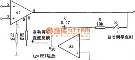
Operational amplifier all-function zero method circuit diagram
Published:2011/6/27 4:53:00 Author:Rebekka | Keyword: Operational amplifier all-function zero method | From:SeekIC

The figure shows the generic auto-zero circuit. A2 is the FET input type integrated chip. The integrator is composed of R, C, etc. It can be integrated to the DC output offset voltage. The switch S is an electronic switch that can automatically achieve the sampling time period. It can make the A1 output offset voltage be used as the input signal. The output points drive the zero end of A1, so that the offset voltage is the minimum state . The resistance of resistors R1 and R2 are larger. The different types of integrated operational amplifier values is around 5MΩ.
Reprinted Url Of This Article:
http://www.seekic.com/circuit_diagram/Amplifier_Circuit/Operational_amplifier_all_function_zero_method_circuit_diagram.html
Print this Page | Comments | Reading(3)

Article Categories
power supply circuit
Amplifier Circuit
Basic Circuit
LED and Light Circuit
Sensor Circuit
Signal Processing
Electrical Equipment Circuit
Control Circuit
Remote Control Circuit
A/D-D/A Converter Circuit
Audio Circuit
Measuring and Test Circuit
Communication Circuit
Computer-Related Circuit
555 Circuit
Automotive Circuit
Repairing Circuit
Code: