
Circuit Diagram
Index 1360
VERY_LOW_FREQUENCY_MULTIVIBRATOR
Published:2009/6/23 22:25:00 Author:Jessie
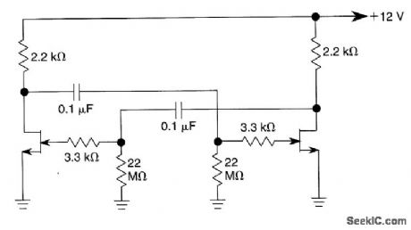
The use of JFETs permits, high resistance and long time constants in this very low frequency multivibrator. The values shown are for 0.15 Hz operation. (View)
View full Circuit Diagram | Comments | Reading(752)
ASTABLE_MULTIVIBRATOR_OR_FREE_RUNNING_SQUARE_WAVE_OSCILLATOR
Published:2009/6/23 22:28:00 Author:Jessie

This free-running square-wave oscillator uses two npn transistors. Output frequency is approximately 300 Hz with the values shown. (View)
View full Circuit Diagram | Comments | Reading(831)
555 long time delay circuit 2
Published:2011/7/29 2:23:00 Author:Ecco | Keyword: 555, long time , delay circuit
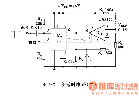

The circuit is shown as the chart 6-2, the delay circuit is a trigger delay circuit with integrator.
CA3140 is a BIMOS single-supply op amp, itcan still work when the value ofVref is very low or zero, and its gate (pin 8)can discharge frompin 7of 555 (through D1). Diode D1is required to the J-FET gate - source PN junction with smaller leakage, the conduction current is high, reverse leakage is small (about 100pA).
As shown in Figure 5-2, the delay circuit is a trigger delay circuit with integrator. When the negative pulse is triggered, the pin 3 is in high level, and pin 7 is in open circuit, then C2R4 integrator makes line integralon the reference voltage Vref = 0.1V divided by the R1, R2.
(View)
View full Circuit Diagram | Comments | Reading(1237)
MONOSTABLE_MULTIVIBRATOR_I
Published:2009/6/23 22:26:00 Author:Jessie
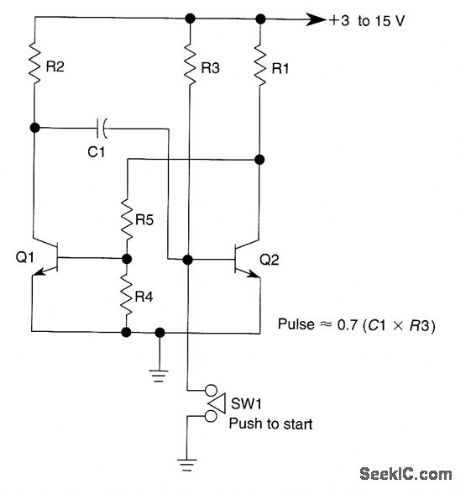
This circuit is activated when SW1 is pushed to ground the base of transistor Q2. The pulse rate is approximately equal to 0.7(R3×C1). (View)
View full Circuit Diagram | Comments | Reading(557)
32_CHANNEL_ANALOG_MULTIPLEXER
Published:2009/6/23 22:19:00 Author:Jessie
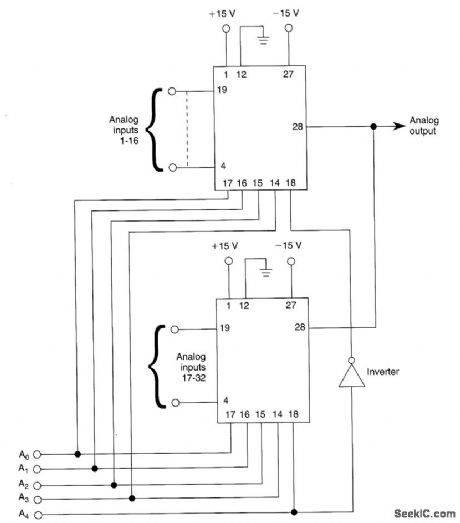
Using two Siliconix DG506 multiplexer chips, this 32-channel analog multiplexer selects 1 of 32 channels, depending on the data inputs A0 - A4. (View)
View full Circuit Diagram | Comments | Reading(1063)
1.8 kHz signal generator
Published:2011/7/29 2:27:00 Author:Ecco | Keyword: 1.8 kHz , signal generator
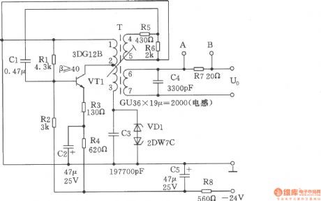
The circuit is shown as the chart, it selects the best working conditions and reasonable temperature coefficient of components in resonant circuit. It also takes Ac regulator measures both ends of the resonance in order to obtain a good output amplitude and frequency stability. Temperature is +25 ℃ ± 20 ℃. The supply voltage changes in the range -40% of -24V, frequency: △ f ≤ 2Hz, the output level: △ dB ≤ 0.26dB.
(View)
View full Circuit Diagram | Comments | Reading(498)
SPEED_CONTROL_SWITCH
Published:2009/6/23 22:15:00 Author:Jessie

The speed-control switch offers reasonably good control and stability to both ends of its operating range. This circuit uses two SCR devices in a full-wave configuration to control the dc power to a motor. A center-tapped transformer is used to supply the SCRs. (View)
View full Circuit Diagram | Comments | Reading(1346)
PULSE_WIDTH_MODULATED_MOTOR_SPEED_CONTROL
Published:2009/6/23 22:09:00 Author:Jessie

Connected in this manner, an LM317 1-A adjustable-voltage regulator can be used to control the speed of a miniature dc motor or vary the brilliance of a small lamp. The circuit does so by controlling the pulse width, and therefore the current, to the load device.
To set the desired maximum output voltage, momentarily close 51 and adjust R3. Connect either a lamp or small dc motor (as is shown in the schematic to the circuit's output) and adjust R4 for the desired results. Atv device that is driven by this circuit should have a current requirement of 1 A or less. And you should be sure to use good-sized heatsink for the LM317 regulator IC. (View)
View full Circuit Diagram | Comments | Reading(971)
PIEZO_MOTOR_DRIVE
Published:2009/6/23 22:06:00 Author:Jessie

Using two Apex Microtechnology PA41 devices in a bridge circuit, this piezo motor driver delivers 0- to 630-V output. (View)
View full Circuit Diagram | Comments | Reading(2291)
SPEED_CONTROL_SWITCH_CIRCUIT
Published:2009/6/23 22:03:00 Author:Jessie

A center-tapped 240-V transformer is used with two SCR devices to provide rectified ac (pulsating dc) to MOT1. Q1 is a UJT ramp generator used to generate trigger pulses for SCR1 and SCR2. (View)
View full Circuit Diagram | Comments | Reading(555)
800Hz signal generator
Published:2011/7/29 2:27:00 Author:Ecco | Keyword: 800Hz , signal generator
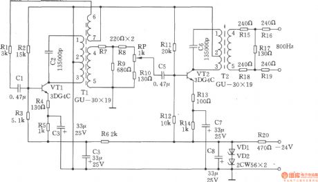
It is a LC oscillator circuit with800Hz oscillation level for the transformer coupled, it's a simple circuit, the frequency is stable. Buffer amplifier isused for reducing distortion, it can adjust the output level by potentiometer. 1. Specifications (1) operating frequency: 800Hz; (2) Frequency stability: ≤ ± 20Hz; (3) Output Level: 0dB/600Ω. 2.Working principle of the circuit is shown as the circuit. 800Hz signal generator is composed of LC oscillator and buffer amplifier. Oscillator: tuned transformer Tl is used as LC oscillation tank and output transformer, C2 is the tuned capacitor. The inductance of oscillation tank is the positive temperature coefficient, and polystyrene capacitor is the negative temperature coefficient, so the compensation of temperature coefficient improve the frequency stability. R2, R3 are DC bias resistors. R4, R5 are the emitter resistors of VTl, R4 has a current negative feedback. C3 is a bypass capacitor R5. R6 and R4 form a decoupling circuit for inter-stage power supply, R7, R8, R9 form the buffer attenuation device; buffer amplifier stage: C5 is the coupling capacitor, R11, Rl2 are bias resistors of VT2, Rl3, Rl4 are the emitter resistors of VT2, C7 is bypass capacitor of R14, C6 and T2 form a tuned output circuit to reduce distortion, RP potentiometer is used to adjust the output level. Buffer amplifier output terminal connecting to a 600Ω attenuation with Rl5 ~ Rl9 could provide 0dB output level. VDl, VD2, R20, C8 constitute regulator circuit.
(View)
View full Circuit Diagram | Comments | Reading(640)
SCM C8051FC40 and FM20L08 Expansion Circuits
Published:2011/7/26 2:05:00 Author:Michel | Keyword: SCM, Expansion Circuits


The monolithic integrated circuit expansion already has many mature examples and this paper will not list again and the above picture is monolithic conrolling FRAM principle circuit.The address signals multiplexing mode is used in the system, so they can produce ALE signal. FM20LO8 itself has latches and it chooses signal CE can not like SRAM and it needs precharging time and the signal produces HC04 and HC32.And the falling edge of address signals needs to lock and save and the expansion is shown as the above picture.
(View)
View full Circuit Diagram | Comments | Reading(592)
PWM_MOTOR_DRIVE_CIRCUIT
Published:2009/6/23 21:56:00 Author:Jessie

This circuit will drive a small dc motor over a wide range of speeds without stalling by controlling the duty cycle of the motor, rather than the supply voltage. (View)
View full Circuit Diagram | Comments | Reading(938)
BLENDER_CONTROL_CIRCUIT
Published:2009/6/23 21:52:00 Author:Jessie

A 10-speed touch-control blender circuit that uses the low-cost LS314 chip by LSI Systems. The 11th touch pad is for power off. (View)
View full Circuit Diagram | Comments | Reading(1756)
MICROWAVE_MOTION_DETECTOR
Published:2009/6/23 21:47:00 Author:Jessie

Operating at around 1.1 GHz, the detector senses field disturbance in the neighborhood of the antenna. The Doppler signal from detector D1 is amplified and drives a power MOSFET switch. The antenna is a short (2 to 3 ) length of wire. (View)
View full Circuit Diagram | Comments | Reading(1972)
12kHz IF oscillator
Published:2011/7/29 2:36:00 Author:Ecco | Keyword: 12kHz , IF , oscillator
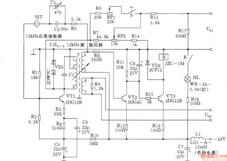
The 12kHz oscillator shown as the chart is composed of 12kHz crystal oscillator, output level adjustment circuit, level rising circuit and the alarm circuit. It employs a novel single-tube tuner variable feedback control oscillation circuit, and in the feedback loop, it connects a 12kHz quartz crystal resonator in series, so that the oscillation frequency depends on the the performance of l2kHz quartz crystal resonators. For improving the reliability and output of the oscillator amplitude stability, it uses AC stable exchange rate circuit, in other respects, the circuit uses the devices with high performance and reliability to obtain excellent performance. Technical characteristics: (1) Nominal frequency: 12kHz; (2) Frequency Accuracy: △ f ≤ ± 0.5Hz; (3) Frequency stability: the temperature is 25 ℃ ± 20 ℃ range, △ f ≤ ± lHz ; (4) output level U01: -40.8dB/600Ω, align the scope: ≥ 3.5dB. Level stability △ dB ≤ ± 0.17dB. When the switch S is closed, U01 level enhances l0.5dB; (5) output level U02: +3.5 ± 0.8dB/1.2kΩ; (6) When the oscillator stops oscillation, there is visible alarm signal.
(View)
View full Circuit Diagram | Comments | Reading(652)
Flyback Synchronous Rectifier Control Circuit of Adapter
Published:2011/7/13 7:51:00 Author:Michel | Keyword: Synchronous, Rectifier Control Circuit


With the development of consumer electronics, energy consumption rate in global electricity of its external power supply(adopter) is dramatically increasing which has been seen as a great energy consumption user.Take America as example, adapters consumes 300 billion degrees electricity per year and it is 11% of the entire country electricity.Today energy conservation and emission reduction is pervasive,at present all governments' regulations are more and more strict to exteral power supply.The United States energy star makes more strict regulations to the average efficiency for external power supply.
Figure 1 shows the power efficency when the output voltage is lagrger than 6V. (View)
View full Circuit Diagram | Comments | Reading(484)
12kHz intermediate frequency signal generator
Published:2011/7/29 1:52:00 Author:Ecco | Keyword: 12kHz, intermediate frequency , signal generator
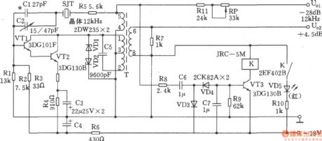
The circuit shown as the chart is composed of l2kHz intermediate-frequency oscillator and alarm circuit. It uses the variable feedback oscillation circuit, and its frequency is determined mainly by the quartz crystal. Cl, C2 can be used for fine tuning frequency. The oscillating tube adopts multiple-unit tube to increase the input impedance, the stability of magnitude could be gotten by bi-directional regulated voltage of VDl and VD2. Specifications: (1) Nominal frequency: 12kHz, the frequency difference does not exceed ± 1Hz; (2) Frequency Accuracy: In the temperature range of 25 ± 25 ℃, ΔF does not exceed ± lHz; (3) U01 output level: -28dB/600Ω, deviation is less than ± 0.2dB; (4) U02 output level: +4.5 dB ± 0.5dB. (View)
View full Circuit Diagram | Comments | Reading(709)
Low Voltage DC Power Charger Circuit
Published:2011/7/22 21:59:00 Author:Michel | Keyword: DC, Power Charge Circuit
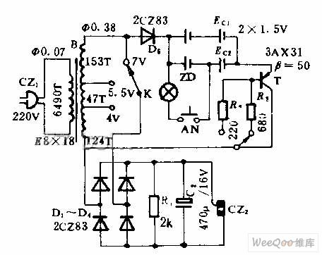
This circuit can be used as nickel cadmium and dry battery's charging and also used as genernal low voltage DC power. This circuit is composed of charging and DC output part.K2 is fast and slow charging choice switch.R2 and R3 are current limitting resistors which can alter charging current value.Usually, quick charging is controlled in 4 h or so, slow charging is about 14 h.NA,ZD consititute test circuit.Please install the batteries which will be charged before the charging.It's normal if the ZD has no light or has slight lihgt when AN is pressed.It's charged fully and can be used by electrical appliances if ZD has sparked for over 10S when the AN is pressed and chagring time meets the requirement. (View)
View full Circuit Diagram | Comments | Reading(442)
JUNKED_TRANSISTOR_REGULATORS
Published:2009/6/23 4:49:00 Author:Jessie

Old transistors can make excellent regulators. Simply use one as a Zener to control the base cur-rent to another transistor (Fig. 68-35A). If the pass transistor cannot supply enough current, you can use two pass transistors in its place (Fig. 68-35B). (View)
View full Circuit Diagram | Comments | Reading(528)
| Pages:1360/2234 At 2013411342134313441345134613471348134913501351135213531354135513561357135813591360Under 20 |
Circuit Categories
power supply circuit
Amplifier Circuit
Basic Circuit
LED and Light Circuit
Sensor Circuit
Signal Processing
Electrical Equipment Circuit
Control Circuit
Remote Control Circuit
A/D-D/A Converter Circuit
Audio Circuit
Measuring and Test Circuit
Communication Circuit
Computer-Related Circuit
555 Circuit
Automotive Circuit
Repairing Circuit