
Circuit Diagram
Index 1345
LOW_VOLTAGE_dc_MOTOR_SPEED_CONTROLLER
Published:2009/6/24 3:27:00 Author:May
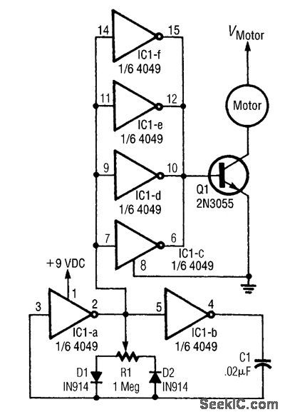
This circuit varies the duty cycle, rather than the voltage. The two diodes control the positive and negative halves of the capacitor's charging cycle. (View)
View full Circuit Diagram | Comments | Reading(587)
TELEPHONE_CALL_RESTRICTOR
Published:2009/6/24 3:34:00 Author:Jessie

This circuit is designed to restrict phone calls with the area codes: 900, 976, and 540. This device uses a microcontroller to compare the DTMF decoded tones with telephone numbers stored in EEP-ROM (IC3). This device requires a programmed microcontroller. Software and details of program-ming can be found in the original magazine article. (View)
View full Circuit Diagram | Comments | Reading(2064)
SYNC_TIP_dc_RESTORER
Published:2009/6/24 3:26:00 Author:May

The dc restorer shown supplies a video signal with sync tips clamped to a baseline level. Clamp drive signal is supplied from elsewhere, usually a sync generator or a sync separator. (View)
View full Circuit Diagram | Comments | Reading(0)
MICROPHONE_AMPLIFIER
Published:2009/6/24 3:34:00 Author:Jessie
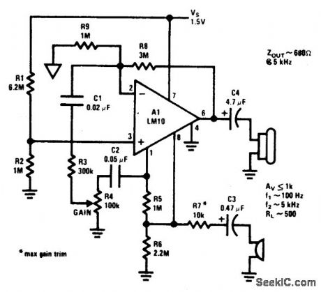
This circuit operates a 1.5 Vdc from source. (View)
View full Circuit Diagram | Comments | Reading(765)
PLD_SYNCHRONIZES_ASYNCHRONOUS_INPUTS
Published:2009/6/24 3:26:00 Author:May

A programmable electrically erasable logic (PEEL) device can easily supply the synchronizing function. Digital systems often require synchronization of asynchronous inputs to avoid the potential metastability problems caused by setup-time violations. A common synchronization method uses two rippled 74LS72 D-type flip-flops.In this circuit, the asynchronous input feeds into the D input of the first flip-flop and its Q out-put feeds into the D of the second. Because the first flip-flop latches on the falling edge of the sys-tem clock, to avoid setup-time violations, the D input signal to the second flip-flop will be stabilized before the rising edge of the clock. Even experienced programmable-logic device designers often re-sort to such a TTL flip-flop circuit to handle the synchronization function, because of the architec-tural limitations of standard PLDs.A programmable elect;ically erasable logic (PEEL) device, such as the PEEL18CV8 from ICT, however, can easily supply the function. The user-programmable 12-configuration I/O macrocells in the device can internally feed back a signal before the output register. With this feedback arrange-ment, designing a two-stage input is simple.A gated-latch internally latches the asynchronous input on the falling edge of the system clock, generating signal Q1. ANDing the input with Q1 through the internal feedback path, eliminates a pos-sible hazard condition during the clock's high-to-low transition time. The latch then holds Q1 stable to ensure meeting the setup-time requirement of the subsequent D flip-flop, which, as before, regis-ters the signal on the next rising system clock edge.If by chance the input pulse width violates the set-up time of the gated latch, the clock's low time will give more time for settling. (View)
View full Circuit Diagram | Comments | Reading(0)
OPTICAL_PROXIMITY_DETECTOR
Published:2009/6/24 3:25:00 Author:May
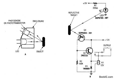
A reflector isolator (A) detects the presence of an object by bouncing light off of it. This tech-nique is useful in circuits that detect when an object is close enough to the sensor (B). (View)
View full Circuit Diagram | Comments | Reading(0)
CALLER_ID_CIRCUIT
Published:2009/6/24 3:33:00 Author:Jessie

This circuit requires programming of the microcontroller. Software information is available from the reference in the original article. (View)
View full Circuit Diagram | Comments | Reading(0)
ULTRA_HIGH_GAIN_AUDIO_AMPLIFIER
Published:2009/6/24 3:33:00 Author:Jessie
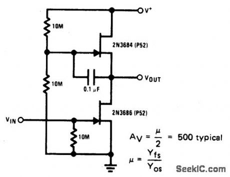
Sometimes called the JFET μt-amp, this circuit provides a very low power, high gain amplifying function. Since pt of a JFET in-creases as drain current decreases, the lower drain current is, the more gain you get. Input dynamic range is sacrificed with increasing gain, however. (View)
View full Circuit Diagram | Comments | Reading(0)
HIGH_SLEW_RATE_POWER_OP_AMP_AUDIO_AMP
Published:2009/6/24 3:24:00 Author:May
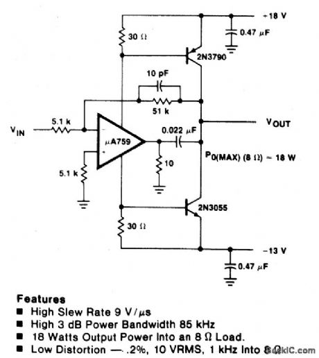
View full Circuit Diagram | Comments | Reading(1138)
ANALOG_SWITCH_CIRCUIT_1
Published:2009/6/24 3:24:00 Author:May

View full Circuit Diagram | Comments | Reading(0)
RADON_MONITOR_AMPLIFIER_AND_HEAD
Published:2009/6/24 3:27:00 Author:Jessie
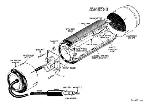
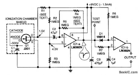
A positively charged anode wire attracts electrons and a negatively charged cathode attracts positively charged ions. The recombination of electrons and ions causes a current that produces a voltage pulse. The cathode is maintained at -500 V by a charge on the 0.1-μF capacitor.A beverage can forms the chamber, an aluminum can forms the cathode, and half cans form protective end covers. The amplifier circuit board is shown to the left of center. (View)
View full Circuit Diagram | Comments | Reading(942)
SIMPLE_SWITCH_DEBOUNCER
Published:2009/6/24 3:23:00 Author:May

Pressing S1 discharges C1 through R1, causing Q1 to cut off, forcing the output high. Once C1 is discharged below the VBE (ON) of Q1, switch bounce will have no effect on the output. (View)
View full Circuit Diagram | Comments | Reading(0)
SYNC_TIP_dc_RESTORER
Published:2009/6/24 3:26:00 Author:Jessie
The dc restorer shown supplies a video signal with sync tips clamped to a baseline level. Clamp drive signal is supplied from elsewhere, usually a sync generator or a sync separator. (View)
View full Circuit Diagram | Comments | Reading(3217)
SWITCH_DEBOUNCERS
Published:2009/6/24 3:22:00 Author:May

These circuits will cure problems caused by switch-contact bounce. The one shown in Fig.88-21A provides you a positive output pulse, and the one shown in Fig. 88-21B provides you a neg-ative output pulse. (View)
View full Circuit Diagram | Comments | Reading(0)
PLD_SYNCHRONIZES_ASYNCHRONOUS_INPUTS
Published:2009/6/24 3:26:00 Author:Jessie
A programmable electrically erasable logic (PEEL) device can easily supply the synchronizing function. Digital systems often require synchronization of asynchronous inputs to avoid the potential metastability problems caused by setup-time violations. A common synchronization method uses two rippled 74LS72 D-type flip-flops.In this circuit, the asynchronous input feeds into the D input of the first flip-flop and its Q out-put feeds into the D of the second. Because the first flip-flop latches on the falling edge of the sys-tem clock, to avoid setup-time violations, the D input signal to the second flip-flop will be stabilized before the rising edge of the clock. Even experienced programmable-logic device designers often re-sort to such a TTL flip-flop circuit to handle the synchronization function, because of the architec-tural limitations of standard PLDs.A programmable elect;ically erasable logic (PEEL) device, such as the PEEL18CV8 from ICT, however, can easily supply the function. The user-programmable 12-configuration I/O macrocells in the device can internally feed back a signal before the output register. With this feedback arrange-ment, designing a two-stage input is simple.A gated-latch internally latches the asynchronous input on the falling edge of the system clock, generating signal Q1. ANDing the input with Q1 through the internal feedback path, eliminates a pos-sible hazard condition during the clock's high-to-low transition time. The latch then holds Q1 stable to ensure meeting the setup-time requirement of the subsequent D flip-flop, which, as before, regis-ters the signal on the next rising system clock edge.If by chance the input pulse width violates the set-up time of the gated latch, the clock's low time will give more time for settling. (View)
View full Circuit Diagram | Comments | Reading(1644)
OPTICAL_PROXIMITY_DETECTOR
Published:2009/6/24 3:25:00 Author:Jessie
A reflector isolator (A) detects the presence of an object by bouncing light off of it. This tech-nique is useful in circuits that detect when an object is close enough to the sensor (B). (View)
View full Circuit Diagram | Comments | Reading(1386)
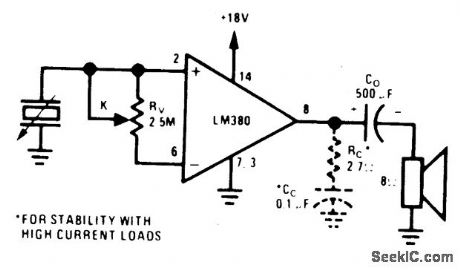
16_W_BRIDGE_AMPLIFIER
Published:2009/6/24 3:25:00 Author:Jessie
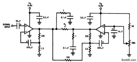
View full Circuit Diagram | Comments | Reading(0)
VOLTAGE_TRIPLER_FOR_RADONDETECTOR_IONIZATION_CHAMBER
Published:2009/6/24 3:22:00 Author:May

The voltage tripler charges the ionization chamber capacitor. It is powered from the 120-Vac line. Warning: Shock hazard exists. (View)
View full Circuit Diagram | Comments | Reading(1070)
HIGH_SLEW_RATE_POWER_OP_AMP_AUDIO_AMP
Published:2009/6/24 3:24:00 Author:Jessie
View full Circuit Diagram | Comments | Reading(0)
PHONO_AMPLIFIER
Published:2009/6/24 3:22:00 Author:May
Used when maximum input impedanceis required or the signal attenuation of the voltage divider volume controlis undesirable. (View)
View full Circuit Diagram | Comments | Reading(533)
| Pages:1345/2234 At 2013411342134313441345134613471348134913501351135213531354135513561357135813591360Under 20 |
Circuit Categories
power supply circuit
Amplifier Circuit
Basic Circuit
LED and Light Circuit
Sensor Circuit
Signal Processing
Electrical Equipment Circuit
Control Circuit
Remote Control Circuit
A/D-D/A Converter Circuit
Audio Circuit
Measuring and Test Circuit
Communication Circuit
Computer-Related Circuit
555 Circuit
Automotive Circuit
Repairing Circuit