
Circuit Diagram
Index 1357
Second-signal circuit (CC4518, CC4001) circuit
Published:2011/7/23 9:28:00 Author:John | Keyword: Second-signal circuit
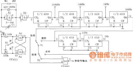
View full Circuit Diagram | Comments | Reading(427)
CC4060 second-signal generator circuit
Published:2011/7/23 9:29:00 Author:John | Keyword: second-signal generator
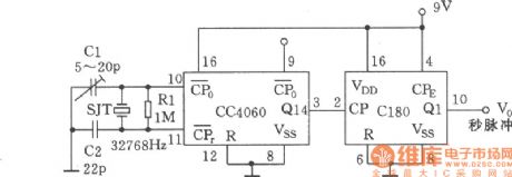
View full Circuit Diagram | Comments | Reading(439)
Multi-phase shift signal generator circuit
Published:2011/7/23 9:29:00 Author:John | Keyword: shift signal generator, Multi-phase shift signal generator
View full Circuit Diagram | Comments | Reading(557)
Southeast Soveran cooling system circuit
Published:2011/7/23 9:29:00 Author:John | Keyword: cooling system
View full Circuit Diagram | Comments | Reading(385)
Southeast Soveran starting system circuit
Published:2011/7/23 9:30:00 Author:John | Keyword: starting system
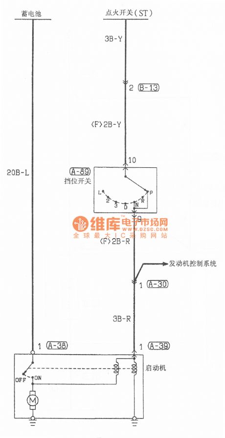
View full Circuit Diagram | Comments | Reading(410)
Southeast Soveran ignition system circuit
Published:2011/7/23 9:30:00 Author:John | Keyword: ignition system

View full Circuit Diagram | Comments | Reading(718)
Linear Circuit of Thermistors
Published:2011/7/22 21:42:00 Author:Michel | Keyword: Thermistors, Linear

The picture is thermistors linear circuit.This circuit is also constant current source circuit and its same phase input port's benchmark voltage is provided by 78LO5.A2 output provides a constant current for thermistors RT and the current enters the ground via R1.Constant current value depends on Rl resistance. If the resistance RT is 5kΩ,the voltage on RT decreases to 0·6V and the constant current is 120 μA. The voltage is added to the VT1 source through the A3 buffer.R2's function is that it makes A3 output voltage keep constant when it flows through invalid current and VT1 source current alters.R3 voltage and temperature on two endsare linear relationship but R3 is float state.Thus,the differential amplifier A4 takes out the voltage and outputs voltage U.It and the temperature become linear relationship. (View)
View full Circuit Diagram | Comments | Reading(728)
Low frequency signal generator(2Hz,4Hz,60Hz,120Hz)
Published:2011/7/29 2:26:00 Author:Ecco | Keyword: Low frequency, signal generator, 2Hz, 4Hz, 60Hz, 120Hz

Low frequency signal generator can be used to measure the sensitivity of amplifier, frequency response, frequency compensation, tone control, it is very useful measuring instruments to repair low-frequency amplifier. It is also used as a digital clock source. Depending on the actual use, the signal generator outputs eight fixed frequencies, selecting switch arbitrarily, the voltage output range can be adjusted in two blocks of 0 ~ 0.1V, 0 ~ 1V. The working principle is shown as the chart. IC CD4060 is a fourteen divider with an oscillator. The crystal SJT produces a 30720Hz weak signal frequency, and it forms a crystal oscillator with Cl and the internal of CD4060 inverter. Rl is used to provide feedback loop, it can only produce oscillation on the fundamental frequency of crystal, the oscillation center frequency is 30720Hz. The tuning capacitor Cl makes the frequency tune at the center frequency. SA is placed at pin 3 of CD4060. 30720Hz is divided by CD4060 nine stage(512 times), the pin 13 outputs high accuracy 60Hz output frequency, the capacitor C3 coupled it to the pin 2 of 741 op-amp for signal amplification, then outputed form pin 6 of 741.
(View)
View full Circuit Diagram | Comments | Reading(2929)
56 ~ 484 khz high frequency oscillator
Published:2011/7/29 1:56:00 Author:Ecco | Keyword: 56 ~ 484 khz high frequency oscillator
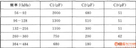
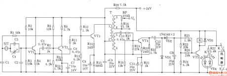
High frequency oscillator is shown as the figure, it can be used as special high-frequency generator, selecting different capacitance between 56 ~ 484 kHz can generate a high frequency. The circuit has the advantages of good shave waveform, high stability of frequency, low output impedance. Selection of components: transistor VTl, VT2: 3DG6D, 65 ≤ β 115, VT3, VT4: 3DGl308, 60 ≤ β ≤ 85. Semi-adjustable capacitor C4: CCWX-3-5/20pF. Crystal SJT: BE-42 type. K: JZX-10M (mini relay). Light-emitting diode VD4: BT-605 (red, green color). Variable device T: using MXD-2000 ferrite, GV-30 × 19 core. Ll-2Φ0.21mm high-strength wire with 133-turn winding, L3-4Φ0.21mm high-strength wire with 11 turns, L5-6Φ0.21mm high-strength wire with 80 turns. Nominal power of resistor uses l/2WRJ models and R27, the other type of resistor are 1/8WRJ. Other parameters of marked element are shown as the chart, there’s no special requirement. The relationship between frequency and capacitor values are shown as below.
(View)
View full Circuit Diagram | Comments | Reading(804)
48MHz HCMOS Oscillator
Published:2011/7/29 2:03:00 Author:Ecco | Keyword: 48MHz, HCMOS, Oscillator
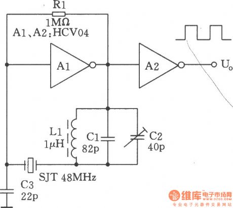
The figure shows the 48MHzcrystal oscillator composed of HCMOS IC. The fundamental frequency of the crystal is l6MHz, butit works in the third harmonic oscillator by force. Harmonic oscillator suppresses the fundamental frequency of the crystal, the parallel resonant circuit in the figure resonances on the base frequenciesof crystal. Connecting to crystal SJT in series may have the highest impedance to fundamental frequency, which can effectively inhibit the fundamental frequency oscillations andensure the third harmonic being easy to start up.
(View)
View full Circuit Diagram | Comments | Reading(1361)
PWM Benchmark Voltage Generating Circuit
Published:2011/7/22 21:41:00 Author:Michel | Keyword: Benchmark Voltage, Generating Circuit

The picture is PWM benchmark voltage generating circuit.In the ciruit,74HC161(1) and 74HC161(2) are four binary counters.Once the clock signal CLK inputs 256 pulses and it outputs、 instructions and trigger 74H04 are set in advance.74 HC191 (1) and 74 HC191 (2) are the subtraction counters.74 HC161 (1) carry instruction makes voltage data load and decreasingly count.4 HC191(1) carry instruction makes the trigger 74HC74 reset and setting and resetting time become relative to their data. Step voltage is lOmV, R2 short-circuits. (View)
View full Circuit Diagram | Comments | Reading(762)
The sine wave oscillator circuit with adjustable frequency, constant amplitude composed of F007
Published:2011/7/29 2:09:00 Author:Ecco | Keyword: sine wave oscillator , adjustable frequency, constant amplitude


Figure shows the sine wave oscillator circuit with adjustable frequency, constant amplitude. The circuit consists of two sub-phase circuit and a linear concatenation of the inverting amplifier. Phase-shifting circuit is the combination of integrated operational amplifier A1, A2 and the RC. Since the phase shift of inverter A3 is 180o, therefore, two phase circuits should also be phase-shifted 180o to ensure that the requirements of the circuit oscillation condition with the total phase shift in 360o.The dynamic resistance of diodes D1, D2 is very high when the voltage being low, so the high-gain inverting circuit ensures the start-up circuit. When the oscillation amplitude rises, the dynamic resistance of D1, D2 getting smaller and smaller reduce the gain of the circuit, so that the output amplitude is stable. Because the diode has a larger dead zone voltage, small signal output waveform has stopped, it is added a resistor R2. The oscillation frequency of the circuit:
Adjusting potentiometer W1 and W2 can change the frequency. As the phase shift circuit has no effect on amplitude, the regulation frequency does not affect the stability of amplitude. W1 can adjust the frequency changing in about 10 times, the scope of its regulatory role is not obvious when over the range, then it can be adjusted by w2.
(View)
View full Circuit Diagram | Comments | Reading(2231)
High Precision PWM Wave Generating Circuit
Published:2011/7/22 21:39:00 Author:Michel | Keyword: High Precision, PWM Wave, Generating Circuit

The above picture is high precision PWM wave generating circuit.This circuit uses the number and data to control the dutyfactor accurately and constantly in 1%~99% range on the basis of 1% step.It can be used as calibration and adjustment PWM demodulation circuit or used as D/A converter sources D/A converter sources in PWM way.74 HC04 inverter and X1 (2 MHZ) constitute the crystal oscillator circuit and its work is very stable and the highest work frequency is 2MHZ.74 HHC190 (1) and 74 HCl90 (2) demodulate and get 20KHZ clock frequency.Once 74 HC190 (2) outputs 100 clock pulse it triggers the bistable multivibrator 74 HC74 one time.Reset method is that using comparators 74 HC85 (1) and (2) 74 HC85 to set.The clock pulse stops counting, circuit resets 74H04 outputs dutyfactor wave which is equal to setting value and the waveform resolution is 1%.
(View)
View full Circuit Diagram | Comments | Reading(1315)
Wideband sine wave VCO composed of LF356N
Published:2011/7/29 2:10:00 Author:Ecco | Keyword: Wideband , sine wave, VCO
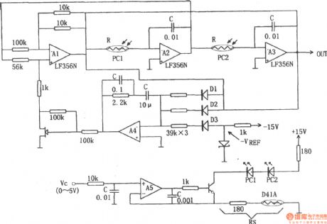
The chart shows the wideband sine wave VCO. Oscillation frequency of the circuit is decided by the resistor R and capacitor C , andthe applied voltage Vc and controlling resistor R constitute theVCO. Variable resistor in the circuit uses photo coupler PC1 and PC2, the rectifier circuit adopts average detection mode. The actual operating frequency of the circuit is tens of Hz or more. In addition, the characteristics of the control voltage Vc with respect to the oscillation frequency depends on the characteristics of optocouplers. The light source of optocoupler is LED and it needs current driving, so the circuit uses the constant current source circuit composed of 4559 operational amplifier. Voltage / current conversion uses Rs, Rs can choose the maximum control voltage Vc freely. In the circuit, IFmax = 30mA, Vcmax = 5V, resistor Rs = 180Ω.
(View)
View full Circuit Diagram | Comments | Reading(1916)
231 Dual amplifier circuit diagram
Published:2011/7/28 3:27:00 Author:Ecco | Keyword: Dual amplifier
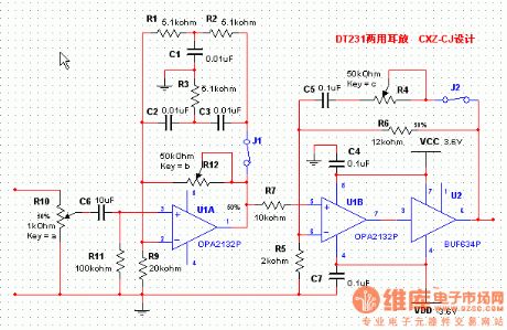
R4 is a low frequency upgrading adjustable resistor replaced by the 12K fixed resistor, and then, it will gradually increase under 100Hz, reach 5-6dB (2 times) under 50Hz, no upgrade above 100Hz. R12 is the If adjustable resistor and replaced by 30K fixed resistors, it makes 2.5-4.5KHz frequency increase, and the band upgrade approximately 6 dB (2 times). If you feel harsh, it needs to add RC, double T decreases. For a fixed resistor, in addition to enhance the band, the circuit overall voltage amplification factor is 3 times, it is enough to push down the headset.J1, J2 are the linkage switch, you can choose generic options or DT231-specific amp. Due toit upgrade little, Q value is not high, the relative frequency change is not great. Due to circuit change little, Q value is not high, the relative frequency change is not great.
(View)
View full Circuit Diagram | Comments | Reading(506)
8_BIT_TRACKING_A_D_CONVERTER
Published:2009/6/24 1:41:00 Author:May

View full Circuit Diagram | Comments | Reading(814)
HIGH_VOLTAGE_POWER_SUPPLY_CONTROL_CIRCUIT
Published:2009/6/24 1:41:00 Author:May


To start the HV supply, S1 is pressed,latching the relay.The 10-kΩ pot is set so that the relayjust latches. When HV current becomes excessive(arc-over,etc.) ,an excessive voltage is developedacross the 10-Ω WW pot,cutting off the 2N3904,causing the relay to unlatch This circuit was used in a 1000-W linear RF power amplifier. (View)
View full Circuit Diagram | Comments | Reading(1063)
Motor Control Circuit of LM339
Published:2011/7/17 10:22:00 Author:Michel | Keyword: Motor, Control, Circuit

The above picture is the motor control circuit composed of LM339 etc.When the input control signal is high PWL,comparator A and A3 make power amplifier conduct composed of A4,VT5 and VT6 and it drives motor M.At the same time,comparator also outputs and removes the armature current integral capacitance C1 reset.The armature current monitors the current enters C1 through A5 and VT3.When RP2 adjustable proportional is constant, the current that enters C1 ,R2 Cl and R3 resistance test armature currentare in proportion.As long as comparator compares the voltage on C1 with RP1 setting voltage,A6 will output high PWL as long as voltage on C1 is lower than RP1 setting voltage. (View)
View full Circuit Diagram | Comments | Reading(3942)
Metal detector 3
Published:2011/7/29 2:45:00 Author:Ecco | Keyword: Metal detector

This metal detectors described in the example can be used as finding location of underground metal pipes, removal and the detection of metal garbage in beach swimming pool and residual nail in wood.The working principle.The metal detector is composed of detection oscillator, reference oscillator and audio amplifier and other components, it is shown in Figure 8-69.
Detection oscillator consists of transistors Vl, V2 and detection coil Ll, capacitor Cl and so on. Reference oscillator consists of transistors Vl, V3 and inductor, capacitor C3 and other components. Audio amplifier audio is composed of power amplifier IC, the volume potentiometer RP and capacitors C6-C8 and so on. Before the end of Ll detecting metal objects, the operating frequency of detection oscillator and reference oscillatorare the same (are aboout 32OkHz), the emitter of V3 has no audio signal output, speaker BL has no sound. When the metal in the ground is detected by Ll, the detection oscillator frequency will become higher, V3 emitter outputs an audio signal, which is amplified by the lC to drive the audio speaker BL, and it issues calls to remind the user metal objects have been detected . (View)
View full Circuit Diagram | Comments | Reading(3791)
8_BIT_A_D_CONVERTER_1
Published:2009/6/24 1:39:00 Author:May

View full Circuit Diagram | Comments | Reading(1002)
| Pages:1357/2234 At 2013411342134313441345134613471348134913501351135213531354135513561357135813591360Under 20 |
Circuit Categories
power supply circuit
Amplifier Circuit
Basic Circuit
LED and Light Circuit
Sensor Circuit
Signal Processing
Electrical Equipment Circuit
Control Circuit
Remote Control Circuit
A/D-D/A Converter Circuit
Audio Circuit
Measuring and Test Circuit
Communication Circuit
Computer-Related Circuit
555 Circuit
Automotive Circuit
Repairing Circuit